I'm not sure how interested folks are in the implementation details but figure I might as well post them in case someone is.
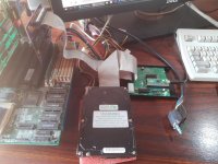
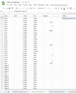
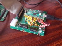
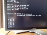
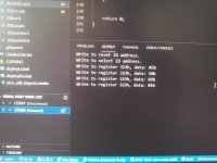
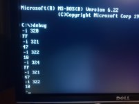
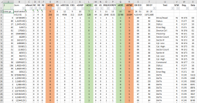
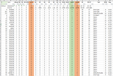
While I wait for boards to come in I have been experimenting with the Raspberry Pi Pico programmable IO. I wrote a couple of logic analyzer type programs to capture what is happening on the bus when the PC is communicating with a real drive. This will run on a slightly modified version of the drive hardware which already has needed signals on the cable connector. One program samples all signals on the bus at high speed and keeps a timestamp. It also filters out any duplicate frames so the Pico memory is not exhausted too quickly. This is for gathering things like precise timing of DMA and IRQ signals. The Pico easily overclocks 2x to 250MHz which gives a 35MHz sampling rate. The other program just makes one capture per read/write so I can capture all of the communications between the PC and drives. This should let me see the communication sequences on my one working drive and I am also interested to see what my two non-working drives do as well.
I have also been doodling with the PIO programs for the actual drive firmware. Mostly just to feel out how they will be implemented and what the final pin connections to the Pico will be. I am pretty sure at this point that I was quite wrong with my earlier statement that a Sound Blaster Pro might be possible with no glue logic. I think an original Sound Blaster would probably be possible with some glue logic. While the PIO is quite flexible and probably Turing complete, the limited instruction set does mean programs tend to be long. I am confident about implementing the 8 bit drives without any additional glue logic however it did take a while to find an approach that will work. Large programs that implement multiple things at the same time use less total instructions however run too slow. Programs that implement single pieces of functionality (like writing to one register) run faster but use more instructions in total. The entire budget on the Pico for PIO is only 64 instructions which is fairly tight. I got kind of lucky that the data register can not be written and read to at the same time, nor even accessed unless the drive indicates it is not busy. This will let me swap between IO read, IO write, IO read DMA and IO write DMA programs for that register. If all of those had to work at the same time I would be in a tough spot.
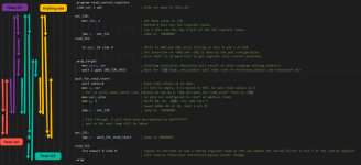
Here is a particularly tricky (untested) example which handles reads from the drive's status register. It is a bit special in that it merges in current IRQ and DRQ pin state with other state bits. The only other palatable way I can think of to implement this would be to use programmable logic.
Optimization of these is challenging and I am always seeing improvements. I have juggled pin assignments numerous times to combine or remove operations. When I pasted this code in initially, read_register_1 was 18 instructions with 18 cycles of read setup time. This was getting close to my calculated maximum of 23 cycles of setup time. Before hitting send I saw improvements and some time later I had it down to 14 instructions and 14 cycles of latency. Then I decided to do this goofy thing to have another program change the Pico pin directions when it sees the bus tranceiver direction change. It increases the overall size of PIO programs by two instructions but reduces latency on all reads by 1 cycle. So now it is down to 13 cycles of read setup time which leaves a large margin of error.
I was not able to implement the functionality where writing to the select register immediately sets busy flags in the status register. Implementing register reads and writes in one program was leading to high instruction counts and high latencies. I also did not have a spare register to efficiently hold the latched busy state. So instead I will dedicate the second CPU core to run a tight polling loop to manage the status flags. I have at least 50 CPU cycles from when the PIO signals the select register to when the status register value needs to be set (time between x86 OUT and following IN instruction). This should be plenty. I would be sweating things a bit on a single CPU micro. The main CPU will have a bunch of other interrupts firing. While none of these interrupts will be particularly time sensitive they could make it tricky to implement a tight polling loop or very fast interrupt handler.
While I wait for boards to come in I have been experimenting with the Raspberry Pi Pico programmable IO. I wrote a couple of logic analyzer type programs to capture what is happening on the bus when the PC is communicating with a real drive. This will run on a slightly modified version of the drive hardware which already has needed signals on the cable connector. One program samples all signals on the bus at high speed and keeps a timestamp. It also filters out any duplicate frames so the Pico memory is not exhausted too quickly. This is for gathering things like precise timing of DMA and IRQ signals. The Pico easily overclocks 2x to 250MHz which gives a 35MHz sampling rate. The other program just makes one capture per read/write so I can capture all of the communications between the PC and drives. This should let me see the communication sequences on my one working drive and I am also interested to see what my two non-working drives do as well.
I have also been doodling with the PIO programs for the actual drive firmware. Mostly just to feel out how they will be implemented and what the final pin connections to the Pico will be. I am pretty sure at this point that I was quite wrong with my earlier statement that a Sound Blaster Pro might be possible with no glue logic. I think an original Sound Blaster would probably be possible with some glue logic. While the PIO is quite flexible and probably Turing complete, the limited instruction set does mean programs tend to be long. I am confident about implementing the 8 bit drives without any additional glue logic however it did take a while to find an approach that will work. Large programs that implement multiple things at the same time use less total instructions however run too slow. Programs that implement single pieces of functionality (like writing to one register) run faster but use more instructions in total. The entire budget on the Pico for PIO is only 64 instructions which is fairly tight. I got kind of lucky that the data register can not be written and read to at the same time, nor even accessed unless the drive indicates it is not busy. This will let me swap between IO read, IO write, IO read DMA and IO write DMA programs for that register. If all of those had to work at the same time I would be in a tough spot.
Here is a particularly tricky (untested) example which handles reads from the drive's status register. It is a bit special in that it merges in current IRQ and DRQ pin state with other state bits. The only other palatable way I can think of to implement this would be to use programmable logic.
Code:
;-----------------------------------------------------------------------------------------
; Register 1 is the flags register.
;
; Note: We must constantly pull from the FIFO to keep the
; register value up to date.
;
; 13 instructions.
; Up to 13 cycle delay to set up data (+ ~4 cycles in external delays)
; Allowed total delay ~27 cycles with 125MHz Pico & 10MHz ISA bus
;-----------------------------------------------------------------------------------------
.program read_register_1
.side_set 1 opt                     ; Side set maps to data_dir
wait_for_read_start:
    pull noblock                    ; Keep read values up to date. If FIFO is empty,
    mov x, osr                      ; X is moved to OSR. So save read values in X.
    ; For 1 cycle lower worst case latency we can do a "jmp pin wait_for_read_start" here on ~IOR.
    mov osr, pins                   ; in pins are configured to start at ~IOR
    out y, 4                        ; Shift ~IOR, ~CS, AEN and A1 into Y (want all 0)
    jmp y-- wait_for_read_start
    out y, 1                        ; Shift A0 into Y (want 1)
    jmp !y wait_for_read_start      ; Jump if A0 not 1

do_read:
    in osr, 2                       ; Shift in DRQ and IRQ still sitting in OSR
    in x, 4 side 1                  ; Shift in the 4 status bits from X and side set tranceiver direction
    mov osr, isr                    ; (Setting tranceiver direction will result in set_pindirs setting pindirs)
    out pins, 8                     ; Set data.
    wait 1 pin 9                    ; Wait for ~IOR high
    irq 3 nowait                    ; Signal to restore pindirs and tranceiver direction.

;-----------------------------------------------------------------------------------------
; Waits for data_dir to go high and then sets pindirs accordingly.
; Waits for interrupt signal before restoring.
;
; in and out pin mappings should be 1 bit starting at data_dir
; set pindir mapping should be 5 bits starting at D0
; side set mapping should be 3 bits starting at D5
;-----------------------------------------------------------------------------------------
.program set_pindirs
.side_set 3 opt pindirs             ; The 3 bits are pindirs for D6-D8
    wait 1 pin 0                    ; Wait on data_dir to go high (pin 22)
    set pindirs, 31 side 7          ; Pindirs set to out for all 8 data bits. 74LVC245 transceiver should have reversed by now.
    wait 1 irq 3                    ; Wait for signal to reverse pindirs / tranceiver direction
    set pindirs, 0 side 0           ; Restore all pindirs.
    mov pins, null                  ; Restore data_dir (tranceiver direction). Must not be before pindirs.
                                    ; Could be at same time however but would require using pindir / pull down to effect this.
                                    ; An option if we end up being an instruction over budget.
Optimization of these is challenging and I am always seeing improvements. I have juggled pin assignments numerous times to combine or remove operations. When I pasted this code in initially, read_register_1 was 18 instructions with 18 cycles of read setup time. This was getting close to my calculated maximum of 23 cycles of setup time. Before hitting send I saw improvements and some time later I had it down to 14 instructions and 14 cycles of latency. Then I decided to do this goofy thing to have another program change the Pico pin directions when it sees the bus tranceiver direction change. It increases the overall size of PIO programs by two instructions but reduces latency on all reads by 1 cycle. So now it is down to 13 cycles of read setup time which leaves a large margin of error.
I was not able to implement the functionality where writing to the select register immediately sets busy flags in the status register. Implementing register reads and writes in one program was leading to high instruction counts and high latencies. I also did not have a spare register to efficiently hold the latched busy state. So instead I will dedicate the second CPU core to run a tight polling loop to manage the status flags. I have at least 50 CPU cycles from when the PIO signals the select register to when the status register value needs to be set (time between x86 OUT and following IN instruction). This should be plenty. I would be sweating things a bit on a single CPU micro. The main CPU will have a bunch of other interrupts firing. While none of these interrupts will be particularly time sensitive they could make it tricky to implement a tight polling loop or very fast interrupt handler.

