glitch
Veteran Member
As I've mentioned a few times, I've got an 8085 project I've been working on for a while. Sometime around last Christmas, I decided to finally build a system around the 8085 processor, something I'd wanted to do since finding an 8085 in an old piece of AT&T PBX equipment. This is what came out of it:
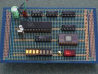
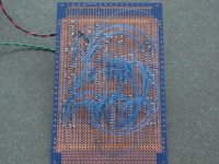
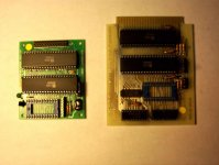
The prototype is entirely point-to-point wired using #30 Kynar wrapping wire. It's got a 2716 2K x 8 ROM for program storage and two 2114 1K x 4 RAMs for stack/variable storage. There's a PDSP-1881 character display mapped to I/O ports 0-3...port 0 is also shared with a TIL311, which was used in the initial testing of the board. There's also a LED attached to the SOD pin of the 8085.
Anyhow, the prototype worked, and I found it to be fairly useful for applications where I wanted to use devices that really needed a full address and data bus -- the PIC uCs I'd been working with only provide ports of varying widths. My 8085 board provided something a lot closer to a true bus-oriented system, and conveniently would run code that could be tested/debugged/run on my S-100 system. I decided to design an etched PCB with some manner of expansion bus for use in other projects. It arrived today, and so it had to be assembled immediately!
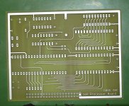
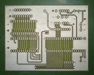
This is the bare board as it arrived today. I ordered a double-sided board from PCB-Pool, which managed to be cheaper than BatchPCB! No silkscreen, no soldermask, only double-sided etch with plate-throughs and electro-less tin coating. Next, we add the sockets and the discrete components:
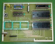
These include the oscillator crystal and its capacitor (lower left), the reset circuit (capacitor, resistor, diode and tact switch in the upper left), the tantalum capacitor serving as main power supply bypass (silver tube top center), and the smaller 0.1 uF bypasses scattered around the board (blue-green beads). There's also a 1Kohm x 5 resistor pack near the bottom of the board, and this holds various interrupt/hold lines down.
[See next post...the forum won't let me upload more than 5]
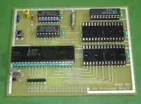
Then the sockets get stuffed with various ICs. The big one is, of course, the Intel 8085. This particular 8085 is the "A" revision, but an actual Intel part. The first IC above the 8085 is a 74LS138, which decodes the top three address bits into 8 select lines for memory devices -- the first two outputs are mapped to the ROM and RAM. The 74LS138 also depends on the 8085's Memory-I/O status line, which keeps the memory devices from responding during an I/O read/write. The IC above that is a 74LS14 Schmitt hex inverter, which forms part of the reset circuit.
The reset circuit itself bears mentioning, as it is simple but effective. It consists of a capacitor, charge resistor, shunt diode and the tact pushbutton. On power-up, the capacitor is discharged due to the diode, so the system is put in reset. It charges through a 10K resistor, allowing for a nice, wide reset pulse. It serves double-duty though, because the tact switch in the circuit will also shunt the capacitor's charge to ground when it closes, so it provides both power-up reset and debouncing/proper pulse width for the reset pushbutton.
The final small IC is the 74LS573, which is an 8-bit-wide latch. This is needed to latch the multiplexed low address bits off of the address/data bus.
[See next post...the forum won't let me upload more than 5]
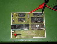
Finally, the RAM and ROM go in. The ROM socket will accept either 2764 or 27128 ROMs, but will only use the first 8K (address pin 13 [NC on the 2764] is tied to ground). I loaded the ROM with a short routine, written in Assembly, to flash a LED on the SOD pin of the 8085:
The code was first tested on the original point-to-point prototype, so I knew the code was good. Fortunately, it worked right-off in the new PCB version:
http://www.youtube.com/watch?v=D1_BuXNkgEM
An overly complicated oscillator!
Why should anyone else be interested in this? Well, I designed the board in Eagle CAD...but I've only got the free version. I kept it within the size constraints so that anyone wishing to build a board to use with this one could do so in Eagle CAD Lite. The bus connector is intended to be a 40-pin IDC connector, so one could attach a 40-pin IDE cable to it, put a right-angle header in it, or put a stacking connector in it. I plan on providing the schematics and board artwork for free, once I get them cleaned up a little. Since it's 8085-based, you can write code for it using classic Assembly tools, such as the Macro-80 compiler under CP/M (I plan on doing a lot of the development with my Kaypro!)


The prototype is entirely point-to-point wired using #30 Kynar wrapping wire. It's got a 2716 2K x 8 ROM for program storage and two 2114 1K x 4 RAMs for stack/variable storage. There's a PDSP-1881 character display mapped to I/O ports 0-3...port 0 is also shared with a TIL311, which was used in the initial testing of the board. There's also a LED attached to the SOD pin of the 8085.
Anyhow, the prototype worked, and I found it to be fairly useful for applications where I wanted to use devices that really needed a full address and data bus -- the PIC uCs I'd been working with only provide ports of varying widths. My 8085 board provided something a lot closer to a true bus-oriented system, and conveniently would run code that could be tested/debugged/run on my S-100 system. I decided to design an etched PCB with some manner of expansion bus for use in other projects. It arrived today, and so it had to be assembled immediately!


This is the bare board as it arrived today. I ordered a double-sided board from PCB-Pool, which managed to be cheaper than BatchPCB! No silkscreen, no soldermask, only double-sided etch with plate-throughs and electro-less tin coating. Next, we add the sockets and the discrete components:

These include the oscillator crystal and its capacitor (lower left), the reset circuit (capacitor, resistor, diode and tact switch in the upper left), the tantalum capacitor serving as main power supply bypass (silver tube top center), and the smaller 0.1 uF bypasses scattered around the board (blue-green beads). There's also a 1Kohm x 5 resistor pack near the bottom of the board, and this holds various interrupt/hold lines down.
[See next post...the forum won't let me upload more than 5]
Then the sockets get stuffed with various ICs. The big one is, of course, the Intel 8085. This particular 8085 is the "A" revision, but an actual Intel part. The first IC above the 8085 is a 74LS138, which decodes the top three address bits into 8 select lines for memory devices -- the first two outputs are mapped to the ROM and RAM. The 74LS138 also depends on the 8085's Memory-I/O status line, which keeps the memory devices from responding during an I/O read/write. The IC above that is a 74LS14 Schmitt hex inverter, which forms part of the reset circuit.
The reset circuit itself bears mentioning, as it is simple but effective. It consists of a capacitor, charge resistor, shunt diode and the tact pushbutton. On power-up, the capacitor is discharged due to the diode, so the system is put in reset. It charges through a 10K resistor, allowing for a nice, wide reset pulse. It serves double-duty though, because the tact switch in the circuit will also shunt the capacitor's charge to ground when it closes, so it provides both power-up reset and debouncing/proper pulse width for the reset pushbutton.
The final small IC is the 74LS573, which is an 8-bit-wide latch. This is needed to latch the multiplexed low address bits off of the address/data bus.
[See next post...the forum won't let me upload more than 5]
Finally, the RAM and ROM go in. The ROM socket will accept either 2764 or 27128 ROMs, but will only use the first 8K (address pin 13 [NC on the 2764] is tied to ground). I loaded the ROM with a short routine, written in Assembly, to flash a LED on the SOD pin of the 8085:
Code:
[FONT="Courier New"];Flash a LED on SOD
;Does not use RAM

FLASH:   MVI A, 0C0h
         SIM
         LXI H, BACK
         JMP DELAY
BACK:    MVI A, 40h
         SIM
         LXI H, FLASH
         JMP DELAY
         JMP FLASH

;Delay, return to HL when done.
DELAY:   MVI A, 0FFh
	 MOV B, A
PT1:     DCR A
PT2:	 DCR B
         JNZ PT2
         CPI 00h
         JNZ PT1
         PCHL[/FONT]
The code was first tested on the original point-to-point prototype, so I knew the code was good. Fortunately, it worked right-off in the new PCB version:
http://www.youtube.com/watch?v=D1_BuXNkgEM
An overly complicated oscillator!
Why should anyone else be interested in this? Well, I designed the board in Eagle CAD...but I've only got the free version. I kept it within the size constraints so that anyone wishing to build a board to use with this one could do so in Eagle CAD Lite. The bus connector is intended to be a 40-pin IDC connector, so one could attach a 40-pin IDE cable to it, put a right-angle header in it, or put a stacking connector in it. I plan on providing the schematics and board artwork for free, once I get them cleaned up a little. Since it's 8085-based, you can write code for it using classic Assembly tools, such as the Macro-80 compiler under CP/M (I plan on doing a lot of the development with my Kaypro!)
Last edited:

