• Please review our updated Terms and Rules here

How to Start hardware of 8085up......??

No maximum limit--a 150 nsec. minimum limit. However, know that when an input needs to be at a high level, it's good practice to tie the input to Vcc through a resistor (2-10K) and not directly.
 
OK, it is working well..!!

However, know that when an input needs to be at a high level, it's good practice to tie the input to Vcc through a resistor (2-10K) and not directly.

I found that all data was high in the chip (past).., so i am connecting 4K7 resistance to ground and i will enter data with DIP switches.
are saying to connect the resistance in both ( -ve and + ve) why??
 
Last edited:
The 28C64 is a CMOS chip. Because of the high input impedance of CMOS inputs, one should never leave a CMOS input "floating"--charges can build up and cause unpredictable results.

Your switches should data lines to ground and you should use pull-up resistors (4K7 is okay) to Vcc. That is the conventional way of doing things.

Yes, i have connected 4k7 resistance to ground should i connect V cc also with some low value resistance or it is just ok??
 
I do not understand why you are using pull-down resistances. This is what I'm saying:
Code:
                         VCC
                          +
                          |
                          |
                         .-.
                         | |4K7
                         | |
                         '-'
                          |
                          +--------------+CMOS input
                       \  o
                        \
                         \.
                          o
                          |
                          |
                         ===
                         GND
 
Yes, i have connected 4k7 resistance to ground should i connect V cc also with some low value resistance or it is just ok??
No, ground or Vcc, not both. As Chuck says, the conventional way is to pull up to Vcc and connect to ground through the switch and that made sense with TTL logic because pulling up drew much less current than pulling down. With CMOS it doesn't really matter, although having the switch common connected to ground instead of Vcc is not only the conventional (although unintuitive to some) way of doing it, it can also have a slight noise advantage in some situations.

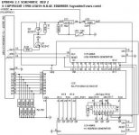
Sounds like you're talking about a manually stepped and programmed version of this parallel-port programmer:

epromr2schem.jpg
 
I know but which program to write in this 2864 and what about RAM 6264 is there any need of it??
First i want to try some basic projects like blinking led from 8085 uP....
 
Well, you should probably map the 2864 EEPROM into the 8085 memory space between 0000h-1FFFh, you could map your SRAM into the memory space between 8000h-9FFFh. Remember that the 8085 will reset to ROM location 0000h. You can then set a stack top at A000h, and you're off and running with your program.

You can implement any sort of I/O, or if you just want to blink a LED, use the SOD pin on the 8085 and the SIM instruction to manipulate it.
 
8085 memory space between 0000h-1FFFh

Why, only 1FFFH not more than this as the memory is of 64KB??
and why, the RAM add. should starts at 8000h to 9FFFh ??
is there any rule for that?
 
The naming convention for EPROMs/ROMs/EEPROMs usually calls out the number of bits, not bytes. A 28C64 EEPROM has 64K bits, organized as 8K 8-bit bytes. So the high address will be 1FFFh.

RAM is usually the same sort of idea. So a 6264 is 8K bytes. There are some exceptions in naming, but it's a pretty good rule of thumb.

But then, you would have known this by reading the data sheets.
 
and why, the RAM add. should starts at 8000h to 9FFFh ??
is there any rule for that?

RAM is usually nessecary for variables and changable data. It just makes things way more practical as you won't have to care about corruption of the original source-data.

There is no rule about where to put the RAM, but 8000h-9FFFh is the simplest solution because it limits the address decoding to only one address line (A15). In such a case, a simple NOT gate is enough for the implemention of address decode for memory.
 
RThere is no rule about where to put the RAM, but 8000h-9FFFh is the simplest solution because it limits the address decoding to only one address line (A15). In such a case, a simple NOT gate is enough for the implemention of address decode for memory.

Not only that, but the scheme leaves room to add more RAM or ROM without having to re-work address decoding. In addition, there's no need to decode any address line but A15, as Per mentions. A0-A12 go to the corresponding lines on the RAM and ROM; A13-A14 are not connected and A15 goes to chip select (negative logic) on the ROM and A15 inverted goes to chip select on the RAM. The contents of ROM and RAM will repeat throughout their assigned address space, but that's usually not an issue.
 
I should also add that a 74LS138 demultiplexer on A13-A15 will provide chip selects every for every 8K block of addresses and speaking from a real-estate point of view, is probably just as efficient.

The advantage offered by partial decoding (using A15) to select between RAM and ROM is that you can expand either ROM or RAM without re-working your address decoding logic.
 
I should also add that a 74LS138 multiplexer on A13-A15 will provide chip selects every for every 8K block of addresses and speaking from a real-estate point of view, is probably just as efficient.

The advantage offered by partial decoding (using A15) to select between RAM and ROM is that you can expand either ROM or RAM without re-working your address decoding logic.

Why A13-A15 pins are not used of 8085 to locate memory in ROM??
as it s said 8085 has 16bit memory add.??
 
Why A13-A15 pins are not used of 8085 to locate memory in ROM??
as it s said 8085 has 16bit memory add.??

Because you have an 8KB device (2864). Since A15 is used to select between ROM and RAM (it's not unused), you can connect up to a 32KB (e.g. M28256) device up for your ROM, if you desire. In that case, A13 and A14 would be used.
 
Because you have an 8KB device (2864). Since A15 is used to select between ROM and RAM (it's not unused), you can connect up to a 32KB (e.g. M28256) device up for your ROM, if you desire. In that case, A13 and A14 would be used.

How you are saying it is 8KB ROM, a 2864 is 64Kb....??
we use RAM to increase processing speed, but how actually it takes Data from ROM and we have to write add........
 
How you are saying it is 8KB ROM, a 2864 is 64Kb....??
we use RAM to increase processing speed, but how actually it takes Data from ROM and we have to write add........

You're playing with me, aren't you?

Note the case of the letter used: "b" = bits; "B" = bytes. 64Kb = 8KB. 2864 = 64Kb = 8KB.

I don't understand the rest of your question, sorry.
 
Back
Top