• Please review our updated Terms and Rules here

New flip chip PCB's

rorypoole

Veteran Member
Joined
Dec 8, 2004
Messages
585
Location
UK, Surrey
I am working on the best way to get a load of pcb's cut and etched to make the flip chips to build my PDP8 straight 8.
I will be only having made flip chip cards made that are used in the PDP8 straight 8, I will have some just cut to size and un-etched, single and double paddle.
I have found a source of cheap dec type handles but only in white for the flip chip copys.
as it costs a lot to get setup a pcb fabrication and the more cards i get made the cheaper each one is, I thought others may want to refill there spears box? or build a PDP8 straight 8? I would like to know if any one is interested in a few cards? I think they will cost about $20 each (not counting postage from England) depending if you want an

un-etched board,
etched board for a certain type of flip chip,
or the same but with modern equivalents components soldered in?
all would come with white dec type handles

the un-etched pcb's could be etched by yourself for any design, all the info you would need is here http://so-much-stuff.com/pdp8/flipchip/flipchip.php

if you are interested reply to this thread with the type and amount you would be interested in, the more the better!


Memory Utilization Module List for pdp8
http://homepage.cs.uiowa.edu/~jones/pdp8/hard8/memmap.html

Processor Utilization Module List for pdp8
http://homepage.cs.uiowa.edu/~jones/pdp8/hard8/cpumap.html
 
Last edited:
I would be interested.

I will send you a PM though when I have had chance to think about it in more detail.

Dave
 
Rory,

I have been "mopping up" and digesting all of the information on the web regarding the PDP straight 8. I have been thinking for a while about construction of a "transistorised" computer and had a preliminary look at the PDP8 at the time - although an appointment with a hospital temporarily put my plans on hold...

My ideal initial solution would be a very basic straight 8 - but using NVRAM rather than core store for the memory (for obvious reasons). I have distilled the module set down the smallest R, S and W set to accomplish this. I think this could be built on "half of a chassis" (i.e. the PROCESSOR half) rather than in two (as in a PROCESSOR and MEMORY chassis). The terminal interface would obviously still be needed from the memory chassis - but this could be moved to occupy slots in the processor chassis.

I then started to look into which cards were really needed, the slot positions and how to wire up the backplane and noticed either accidental or deliberate errors and/or omissions within the DEC schematic diagrams. For example, the schematics I found in one of the maintenance manuals did not agree with the slot maps given in the same maintenance manual! Looking at the schematics themselves also gave me cause for concern that errors were present - which would lead to wire-wrapping errors when making the backplane which would lead to a lot of debugging to get the system to work.

Also of concern was the component availability. So, this is how I would propose to proceed:

1) Identify what flip-chip cards are required to construct a minimal basic straight 8.
2) Construct a SPICE model for each identified flip-chip module using DEC part numbers.
3) Identify suitable modern replacement components and develop the SPICE component models for the identified devices.
4) Test each SPICE module within a test harness to ensure they work.
5) Analyse the schematic diagrams and determine a backplane wiring scheme that can be documented and automatically tested (by software) for sanity. I would propose to use SPICE for this - although actually making a complete working SPICE model of the straight 8 would be beyond sense!
6) Develop the PCB's required and construct the cards.

As I have stated, I believe I have already identified a minimal module set (will post later on).

I have already started to model the modules in SPICE. I have probably got about 80% through this. I have only constructed the test harness for two of the simplest modules so far (S107 and S151) - but the results look promising.

I have started to look into component availability. The resistors and capacitors don't present a problem. Modern diodes look to be easily available but some of the transistors are proving elusive. I will have to try and track down the specifications for the original DEC devices and take it from there.

I have already started to look at simulating the collection of modules forming the terminal interface - so I will let you know how I get on.

Electronic PCB artwork for most of the flip-chip PCBs appears to be available for non-commercial use (see "http://so-much-stuff.com/pdp8/flipchip/Sxxx.htm"). I have downloaded the "free" version of Eagle which allows you to look at these designs - but not change them. To change them will involve purchase of the Eagle package. Before running some of these PCB's through for production however - it would be prudent to check that the schematics and layout of each module agrees with the SPICE model and that the layout is compatible with the modern components available and make changes where necessary.

White card handles appear to be available (without any card ID on them of course). I went to the Gadget show at the NEC last week and went specifically to have a look at 3D printers. I believe that it should not be that difficult to develop the 3D graphics for the DEC handles - complete with the embossing for the card ID - and print them out in either red or white plastic to suite.

The only item I am not sure about at the moment is the edge connector for the backplane. I have found a source in the States - but they don't seem to be the same as was originally used and don't look deep enough to me to accommodate the gold-plated edge connector of the flip-chip fully. I will ask a question regarding this.

What are your thoughts?

Regards,

Dave


I thought I would include a SPICE sample for the S151 for your information...

I hope this turns out sensibly! I have selected a courier font so I will cross my fingers!

Dave


PDP8_S151.cir

* ***************************************************************
* *** ***
* *** Module S151 [Design Rev C] (Binary to Octal Decoder). ***
* *** ***
* ***************************************************************
*
* Version :
* Date :
* Author :
* Change :
*
* Version : 1.00
* Date : 1st April 2013
* Author : Dave Roberts
* Change : First creation.
*
.SUBCKT S151 A B C D E F H J K L M N P R S T U V
*
* *******************
* *** ***
* *** CONNECTOR ***
* *** ***
* *******************
*
* A - +10V
* B - -15V
* C - GND
* D - Common (GND)
* E - 2^1 (0)
* F - 2^1 (1)
* H - 2^2 (1)
* J - 2^2 (0)
* K - 2^0 (0)
* L - 2^0 (1)
* M - Out 0
* N - Out 1
* P - Out 2
* R - Out 3
* S - Out 4
* T - Out 5
* U - Out 6
* V - Out 7
*
* ****************
* *** ***
* *** DIODES ***
* *** ***
* ****************
*
* N+ N- Type
D1 J N103 D664
D2 E N103 D664
D3 K N103 D664
D4 J N106 D664
D5 E N106 D664
D6 L N106 D664
D7 J N109 D664
D8 F N109 D664
D9 K N109 D664
D10 J N112 D664
D11 F N112 D664
D12 L N112 D664
D13 H N115 D664
D14 E N115 D664
D15 K N115 D664
D16 H N118 D664
D17 E N118 D664
D18 L N118 D664
D19 H N121 D664
D20 F N121 D664
D21 K N121 D664
D22 H N124 D664
D23 F N124 D664
D24 L N124 D664
*
D25 N128 M D664
D26 N128 N D664
D27 N128 P D664
D28 N128 R D664
D29 N128 S D664
D30 N128 T D664
D31 N128 U D664
D32 N128 V D664
*
D33 N102 N103 D662
D34 N105 N106 D662
D35 N108 N109 D662
D36 N111 N112 D662
D37 N114 N115 D662
D38 N117 N118 D662
D39 N120 N121 D662
D40 N123 N124 D662
*
D41 C N125 D662
D42 N125 N126 D662
D43 N126 N127 D662
D44 N127 N128 D662
*
D45 N101 N102 D662
D46 N104 N105 D662
D47 N107 N108 D662
D48 N110 N111 D662
D49 N113 N114 D662
D50 N116 N117 D662
D51 N119 N120 D662
D52 N122 N123 D662
*
* *******************
* *** ***
* *** RESISTORS ***
* *** ***
* *******************
*
R1 A N101 100k
R2 A N104 100k
R3 A N107 100k
R4 A N110 100k
R5 A N113 100k
R6 A N116 100k
R7 A N119 100k
R8 A N122 100k
*
R9 B N103 15k
R10 B N106 15k
R11 B N109 15k
R12 B N112 15k
R13 B N115 15k
R14 B N118 15k
R15 B N121 15k
R16 B N124 15k
*
R17 B M 3k
R18 B N 3k
R19 B P 3k
R20 B R 3k
R21 B S 3k
R22 B T 3k
R23 B U 3k
R24 B V 3k
*
R25 B N128 1.5k
*
* ********************
* *** ***
* *** CAPACITORS ***
* *** ***
* ********************
*
* N+ N- Value
C1 C N128 0.01uF
*
* *********************
* *** ***
* *** TRANSISTORS ***
* *** ***
* *********************
*
* Nc Nb Ne Type
Q1 M N101 D DEC3639B
Q2 N N104 D DEC3639B
Q3 P N107 D DEC3639B
Q4 R N110 D DEC3639B
Q5 S N113 D DEC3639B
Q6 T N116 D DEC3639B
Q7 U N119 D DEC3639B
Q8 V N122 D DEC3639B
*
.ENDS S151

* *************
* *** ***
* *** END ***
* *** ***
* *************

TEST_S151.cir

PDP straight 8 simulation of module S151 (Binary to Octal Decoder)
*
* Modification History (latest at the top please).
* ================================================
*
* Version :
* Date :
* Author :
* Changes :
*
* Version : 1.00
* Date : 03rd April 2013
* Author : David E. Roberts
* Changes : First Creation.
*
* ========================
* Ground is always node 0.
* ========================
*
* ===========================
* Define the supply voltages.
* ===========================
*
VPlus10 P10 0 DC +10V
VMinus15 M15 0 DC -15V
VNC NC 0 DC 0V
VGND GND 0 DC 0V

.INCLUDE ../PDP8/PDP8_COMPONENTS.cir

.INCLUDE ../PDP8/PDP8_S151.cir

VIN200 V200 0 DC -3V PWL( 0.0ms -3V 0.9ms -3V
+ 1.0ms 0V 1.9ms 0V
+ 2.0ms -3V 2.9ms -3V
+ 3.0ms 0V 3.9ms 0V
+ 4.0ms -3V 4.9ms -3V
+ 5.0ms 0V 5.9ms 0V
+ 6.0ms -3V 6.9ms -3V
+ 7.0ms 0V 7.9ms 0V
+ 8.0ms -3V )

VIN201 V201 0 DC 0V PWL( 0.0ms 0V 0.9ms 0V
+ 1.0ms -3V 1.9ms -3V
+ 2.0ms 0V 2.9ms 0V
+ 3.0ms -3V 3.9ms -3V
+ 4.0ms 0V 4.9ms 0V
+ 5.0ms -3V 5.9ms -3V
+ 6.0ms 0V 6.9ms 0V
+ 7.0ms -3V 7.9ms -3V
+ 8.0ms 0V )

VIN210 V210 0 DC -3V PWL( 0.0ms -3V 1.9ms -3V
+ 2.0ms 0V 3.9ms 0V
+ 4.0ms -3V 5.9ms -3V
+ 6.0ms 0V 7.9ms 0V
+ 8.0ms -3V )

VIN211 V211 0 DC 0V PWL( 0.0ms 0V 1.9ms 0V
+ 2.0ms -3V 3.9ms -3V
+ 4.0ms 0V 5.9ms 0V
+ 6.0ms -3V 7.9ms -3V
+ 8.0ms 0V )

VIN220 V220 0 DC -3V PWL( 0.0ms -3V 3.9ms -3V
+ 4.0ms 0V 7.9ms 0V
+ 8.0ms -3V )

VIN221 V221 0 DC 0V PWL( 0.0ms 0V 3.9ms 0V
+ 4.0ms -3V 7.9ms -3V
+ 8.0ms 0V )

XS151 P10 M15 GND GND V210 V211 V221 V220 V200 V201 OUT0 OUT1 OUT2 OUT3 OUT4 OUT5 OUT6 OUT7 S151

.TRAN 0.1ms 10ms

.SAVE V(V200) V(V201) V(V210) V(V211) V(V220) V(V221) V(OUT0) V(OUT1) V(OUT2) V(OUT3) V(OUT4) V(OUT5) V(OUT6) V(OUT7)

* ========
* The end.
* ========

.END

 
So so...

Multiple spaces seemed to be truncated to a single space so some of the formatting has been lost - but it still seems readable.

Dave
 
I only vaguely understand the SPICE sample? and I am planing on having the full pdp8! then extended pdp8!! I think you are a lot more organised and professional than me! and cant wait to see how you get along.
I am starting the project from the easiest problem first, first I am working on the flip chips, building or buying them, and finding other parts, I have some old diode and transistor equivalents books and have got some modern cheap components that I think are close enough to work, some dec transistors are on ebay but it would cost too much for me to use them for my build.

I also found the site selling White card handles and edge connector for the backplane in the usa, I am planing on buying a sample and testing them, I have got some m type flip chips but they are not the right sort for the fpp-12A floating point processor so I will be trading them, and the white card handles can be painted? a 3d printer is an interesting idea, but I could try casting a copy of the white handles, but plastic would last longer?

I have the first part of my pdp8 build a R111F flip chip! and I am trying to get some more, I want to keep the pcb artwork the same but use nos/used/modern cheap components.

I need to build some sort of flip chip tester to compare the original flip chip to the copy's.

in the UK there are 3 maybe 4 pdp8 straight 8's and I am trying to get asses to one of them so I can copy the steel frame and case and when I need to the backplane wiring!!!

Vincent from so-much-stuff.com has some of the flip chips maked as type x, they use more modem components but are untested.
 
Last edited:
In case you're not aware of it, quite a few people with DEC/PDP knowledge and experience hang out on the CCtalk/CCtech mailing list; maybe there'd also be some interest there, as well as perhaps helpful ideas (if you can wade through the noise...)
 
In case you're not aware of it, quite a few people with DEC/PDP knowledge and experience hang out on the CCtalk/CCtech mailing list; maybe there'd also be some interest there, as well as perhaps helpful ideas (if you can wade through the noise...)

thanks can you post a link
 
I have got 500cl of Ferric Chloride and an Anti-etching PCB Ink Marker Pen in the post, and am going to have a go at making a R111F flip chip
 
This is where I am so far with my SPICE modelling (assuming the image turns out - my first image post).

Scope.jpg

The advantage of using SPICE (the version I use is free) is that you can simulate what would happen inside a PC without initially buying the components. You can try different components until you find devices which appear to perform the function you require. Any modern NPN or PNP transistor will probably do for the digital type of R and S cards (e.g. BC556 and BC546) but the pulse type circuits and flip-flops that use capacitive coupling may take some experimenting.

After I get a working SPICE model, I then purchase some sample components and perform a bench test and compare the results with the SPICE model to ensure that things are as expected.

I will look to add the models for the outstanding flip-chips over and above the basic system shortly.

Ferric chloride and pens - now that takes me back to when I was a trainee!

Dave
 
I have never made a PCB before! in the past I used strip board, and in a few cases a wooden board and copper coated nails or brass tacks, I have already bought a load of semiconductors, I will have to see if I will have to resell them, some flip chips may not be that fussy, some germanium transistors and diodes are needed, the diodes can probably be substituted with Schottky diodes, but the germanium transistors are a problem, there are some bulk NOS germanium transistors on ebay that are cheap, but I dont think they match well.
 
A few things you should consider then to preserve your sanity!

My research has led me to believe that a DEC3639 (equivalent 2N3639) is a SILICON device and not germanium.

You should be able to use any good modern transistor of the appropriate type in the digital modules - but I would like to bet that the flip flops, delays and clocks may be a bit more pedantic.

The initial critical components are the diodes and capacitors.

D664 replaced by 1N4154
D662 replaced by 1N914

The D662 diodes are used for their forward voltage drop to give a stable voltage drop.

For the low-valued capacitors (e.g. 82pF used in some of the flip-flops) I would suggest silver-mica. You will probably not get away with "junk-box" components here otherwise the pulses will go "out of the window"!

I would suggest ceramic disk capacitors for all of the decoupling - and I would probably go for tantalum bead for the uF smoothing capacitors. A bit more expensive than electrolytics but less hassle, smaller and prettier!

If you plan to use a pen as an etch-resistant coating then you may go crazy making each board separately. Much better would be to look for UV sensitive film and transfers. This was the method I started to use after my one (and only...) PCB with a pen! You can buy transfers, tape and transparent drafting sheet. You design the PCB on the drafting sheet using the transfers and stick-down tape (with a scalpel purchased from a model shop or Maplins) and then use a UV light box (can be made yourself if cost is an issue) to transfer the artwork to the UV sensitive film. Develop the film and you have a very robust master that you can use for mass producing your PCBs. Use UV sensitive coated PCB material. You could (in theory) draw on the drafting sheet with a black pen if you want - providing that it is UV opaque. You could also use FreePCB to design the artwork on a PC and transpose this onto UV sensitive film again for a much more professional finish.

The drawback you will have if you make the PCBs yourself will be that you will have to solder the components in almost immediately otherwise the copper will start to tarnish. Normal PCB's will have a tin-plated finish so they will not tarnish so easily. The other issue will be what to do with the edge connector. This would normally be hard gold plated. The chemicals used for this are incredibly dangerous so I would not even contemplate this myself! Without the gold plating, the bare copper edge connector will tarnish and you will have all sorts of reliability problems with the cards due to bad connections.

I don't want to put you off doing this work yourself - but believe me this step may be more work and heartache than you may be thinking at the moment.

Dave
 
I plan to just make a few prototype flip chips and tin the edge connector, not perfect but will work, I have used copper strip board that has been stored open for 20+ years, with no problem, I just give it a clean before soldering it.
the problem with the 2N3639 is that its a 500mhz transistor, I will try out some slower ones with the same or lower capacitance http://alltransistors.com/transistor.php?transistor=3429

some of the flip chips I will need a lot of them like the R111, I will need 42 plus a few spares, but others like the R113 I will only need 1, so I will probably need the make the flip chips that only a few are needed, and pay to have the more used flip chips pcb made up.

also need

for PT08 (for com ports)
10 R401, 5 W005, 5 W070, 10 W103, 5 W705, 5 W706, 5 W707

for FPP-12A floating point unit
M107 M127 M133 M135 M139 M155 M172 M178 M190 M191 M205 M238 M245 M611 M734
dont know how meny flip chips needed but need to get pdp8 built and working first

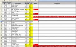
how do you upload a spreadsheet?
 
Last edited:
I will have to think about what to say on CCtalk?

for full pdp8
42 R111, 28 R603, 20 R002, 17 R650, 17 W011, 14 W024, 14 R107, 13 R210, 13 G007, 12 R211, 12 B684, 11 R602, 9 R203, 8 R202, 8 W026, 8 G209, 7 R205, 7 G208, 6 R212, 6 R201, 6 R220, 5 R123, 5 R302, 4 R151, 4 W640, 4 R181, 4 B130, 3 R405, 3 A604, 3 W025, 2 W501, 2 R284, 2 R121, 2 R401, 2 A601, 2 W300, 2 B104, 2 B360, 1 R113, 1 W005, 1 A502, 1 A704, 1 G008, 1 W607, 1 B602, 1 B204, 1 W050, 1 W070,

That's still a ton less than the KA-10 project I have planned (but mainly to redraw the schematics) to be able to make
a replacement backplane. To actually make that and the replacement flip chips would cost a small fortune. I don't even
want to think about how many Dec backplane modules would be needed.

48 B130, 45 B133, 60 B134, 45 B135, 40 B136, 40 B137, 60 B138, 25 B141, 4 B152, 31 B156, 89 B163, 85 B165, 9 B166
31 B167, 113 B168, 2 B198, 1 B199, 20 B204, 136 B212, 12 B250, 96 B311, 5 B312, 144 B611, 26 B684, 39 G700, 15 G704
1 G903, 7 R001, 10 R002, 9 R201, 16 R220, 8 R302, 5 R303, 2 R401, 1 R450,1 R601. 7 R602,14 R613, 22 S107
18 S111, 19 S202, 22 S203,, 3 S205, 4 W002, 12 W005,8 W010,5 W040, 10 W102, 3 W501, 2 W504,1 W510,1 W520
1 W602, 1 W990

some of the flip chips are the same type as I will be using!
where will you get all the backplane connecters! I am struggling to find enough at a good price for the pdp8!
 
Last edited:
There are two sources I have located.

www.douglas.com - although they retail for USD 9-40 apiece + UK rip-off-tax + Royal Mail bigger rip-off for them paying the import duty and VAT! I do not know at the moment if these connectors will accommodate the full height of the gold-plated edge connector or not. I have asked a question of them. I also don't know what stock they have in total.

I may have located some locally in the UK from "http://www.in2connect.uk.com/sullins_connectors.html". We use this company a lot so I will contact them to see if I can have a sample and what would be the best price they could do for me in bulk...

If you already have a "real" straight 8 board I would happily send the test connector on to you for testing.

Dave
 
some of the flip chips are the same type as I will be using!
where will you get all the backplane connecters! I am struggling to find enough at a good price for the pdp8!
I know many are the same. I have no plans to actually build this, just to eventually draw it so it can be
layed out in Eagle so if someone else wants to do it they can. To me it would be cost prohibitive. I can't imagine
find that many backplane connectors and actually having the backplane replacement fabbed.
 
Back
Top