• Please review our updated Terms and Rules here

MORE on DMA controller

Don't worry about being puzzled, I'm often puzzled and I made the thing. By behind the buffers, do you mean between the 8080 and address buffers? If the 8237 was there, the 8237 address lines would be cut off from memory also. This way the buffers are driving everything on the address bus so the 8080 doesn't have to. I have the MCS-80 manual and my circuit is similar except the address buffers are between the 8080 and the "T" in the address lines to the 8237 (8257 in the picture). I suppose it's all in what you are used to. Seems the simple controllers that I made many years ago were all 8085's yet the prototyping was done on this 8080A and this is all that I have left.
Mike
 
You've got the idea--the 8080 address lines and the 8237 lines are tied together and then off to the bus through the buffers. The idea is that you have tight coupling and no timing/handshake issues between the two. Now, I'm just thinking aloud, so you probably shouldn't take that for much.

In any case, what you're saying is that the DMA cycle ensues, but then you get a spurious memory reference at the end of the cycle?

Or am I not understanding what you're saying?
 
No, the errors are not spurious. For example say the DMA transfer is set to transfer 128 bytes to address 100 000 (base 8). The completed transfer should have preset data in address locations from 100 000 to 100 200. Well.... for the most part it does, but My console Uart has an I/O address of 070, and 071. When I look at the DMA transferred data, in locations 100 070 and 100 071, the preset data is not there, something else is. It turns out the Console Uart responded and inserted it's data here, because the DMA address and the I/O R signal selected the Uart. I also have another Uart, two parallel ports, one timer and a interrupt controller. At each I/O address for each of these I/O devices, I do not have the preset data from the DMA transfer, I get something from each of the I/O devices. So, that is why I think Pearce is correct, I need to "AND" the HOLD ACK with the device select address decoding for these I/O devices. Then when the CPU is holding and the DAM transfer occurs, the other I/O devices can not respond.
Do you smell what I'm stepping in?
Thanks Mike
 
So what you're saying is that during the DMA, the UART gets selected by a memory (not I/O) address and brute-forces the data bus. This is in an I/O to memory transfer? So IOR/ is being asserted during that time--and MEMW/?
 
Last edited:
What I think is occurring is, During a DMA write (peripheral to Memory), the DMA address is placed on the bus and when that address is the same as an I/O device address, the I/O R causes the Uart or other I/O device to respond. The DMA simultaneously accesses memory and I/O, so when the Memory Address is issued, it also is applied to the I/O Device select address decoding. That address and the I/O R causes the I/O device two respond.
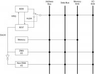
Thinking more about what you were saying about where the DAM controller should be, If the DMA controller is behind the address buffers, Memory would also have to be behind the buffers. The I/O devices would be on the other side of the buffers.View attachment DMALocation.pdf
Which setup are you referring to? My machine is wired like the blue.
Mike
 
Forget what I said--the IBM 5150 gets along perfectly well with the DMAC and memory on the far side of the buffers.

I assume that you've programmed the DMAC for single/demand mode.

Would it be possible to see the schematic of your DMAC board? I looked on this thread and can't find it--just the CPU board.
 
Well..... I just added a Hold Ack signal S-26 to the address decode device select for my console Uart and this works. If the DMA transfer address is 100 000, prior to the change I would get some non preset data at addresses 100 070 and 100 071. My console Uart data I/O address is 070 and the status address is 071. So I believe that this approach would correct the problem.

Yes the DMA is programmed for single transfer. I didn't post the DMA schematic. I can post it a little later today. I started to look at the XT manual, but haven't satisfied myself.

Thanks
Mike
 
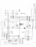
Here is part of my DMA schematic. I really have a hard time making a JPG or PDF that is legible. I hope you can make it out.
Thanks
Mike
DMAx.jpg

Seems that this forum must compress the images. I started with 500K and now that it is here it is less than 100K. Don't know why.
Mike
 
I spent some time looking at the IBM Tech Ref for the XT. Sheet 1 page 1-47 shows the bus controller where the I/O R&W and the MEM R&W are made. If you go to Sheet 5 page 1-51, at the bottom left there is a ls 243 chip where these signals go into. This is a bi direction buffer. The outputs are called XI/O R&W and XMEM R&W. The gate control is the DMAAEN. The XI/O R&W go to the timer 8253 and parallel port 8255, etal. I have not completely analyzed this, but it looks like the DMA does condition these signals to the I/O devices.
Thanks
Mike
 
Mike, I'm not sure how you're doing your schematics. Are they hand-drawn? If not, why not just post the individual sheets and I can paste them together here. I'm going blind trying to read them.

Basically, your setup should be DMA controller asserts HRQ on the 8080A HOLD pin, the 8080A responds with HLDA to the HLDA pin on the DMAC. At this point the CPU address buffers should be tristated using the AEN output of the 8237 which also enables the address latch tristate control for the DB0-DB7 outputs. The upper address byte is then latched by the 8237 ADSTB signal. The lower 8 address bits of the 8237 can be buffered, with the tristate control again controlled by (the complement) AEN. Thus, depending on AEN from the 8237, either the address lines from the 8237 or the address lines from the 8080A are enabled. Note that the AEN output from the 8237 (according to my datasheet) controls which device (the 8237 or the 8080) has the bus (HLDA extends somewhat before and after AEN, but should not be used as a tristate control). Note that the entire read/write of a single byte with addresses happens under the envelope of AEN, including the bus MEMR, MEMW, IOR and IOW signals. AEN goes high exactly one cycle after HLDA is asserted by the CPU.

In other words, 8237 AEN says which chip (8237 or 8080) is driving the bus.

Does this follow your understanding?
 
Last edited:
I'm sorry that the prints clarity stinks. I can try the page method. I agree with what you are saying (above). My point is that no matter which device issues an address on the address bus, all I/O and memory will see that address. At least in my case all I/O and memory are on the 'far' side of the address bus buffers. Either I have to segregate the I/O signals or use the DMA Ack signal to prevent the I/O response.
Thanks
Mike
 
What are you using for address decoding? If you use a 688, its gate can be simply connected to AEN as happens in the PC.

Chuck is I'm sure right on the timing - I thought that the IBM PC AEN was generated from the HOLDACK, but see this is actually generated by the 8237 itself, which of course should be sufficient.
 
My address decoding is very simple. I use some inverters and an 8 input NAND for each I/O device. When the 8080 issues a I/O address it places an 8 bit address on the low 8 bits of the address bus and the same 8 bits on the high 8 bits of the address bus. So my I/O address decode only looks at the low 8 bits of the address bus.
Actually I didn't use the AEN, I connected the HOLD ACK the the 8080 issues to the 8237 and applied this signal to one of the inputs of the 8 input NAND's that decode the I/O addresses. I have tried this with one of my I/O devices and it works. I'm going to add this signal to the other I/O devices. This should resolve the problem. I hope I didn't cause Chuck any permanent eye damage. I keep prints of this machine, but use an old DOS version of OrCad and it only allows my to make hard copy output rather than files. I'd like to get it to make a PDF or some other file output, but......
Thanks
Mike
 
Mike, what platform are you running your OrCad on? If it's NT or one of its sisters, you can create a printer port that outputs as a PDF file. I run a couple of old QBASIC programs that way and it works a treat.

Unless my memory fails me, the OldDOSOrcad Yahoo! group has an old copy of Windows 3.x in its files section, which may provide some additional flexibility.

I'm an old TangoSDT user (and before that, Schema run on a 5160), so I am aware of the problems that occur, particularly when you're trying to print a D-sized drawing.

I'm not entirely sanguine about using HLDA as part of the I/O address decoding, mostly out of my bias that that's not its purpose.

However, the lack of the proper signal lines on the S100 bus does explain why using an asynchronous master like an 8237 creates such a problem--there's no way to pass along the handshaking protocol. Multibus I can do it, but again, it's not easy.
 
The OrCad I'm using is a DOS version 3. I'll look up the sites you mention. Maybe I can use some of that stuff.

The Hold ACK works, but that doesn't mean it's correct or right. I want to understand this better, I have some other program updating to do, mean while I keep thinking about this and maybe I can find out the "way".

Thanks for all the help and discussion.
Mike
 
You might want to think about it this way--the 8237 is a close relative to a second CPU in your box. Another CPU could just as well plug into the bus, assert HOLD, wait for HOLD_ACK and assume control of the status and address lines. I think if you think about things this way, you may gain some inspiration. That's why I initially suggested putting the 8237 on the same card as the 8080A, so that the decision of who gets control of the bus might be worked out before the bus, rather than after.
 
Normally the CPU has control of the Address, Data and Control Busses (Memory & I/O R/W). When the DMA controller requests a HOLD, when the CPU can it will issue a HOLD ACK and transfer control of the busses to the DMA Controller.

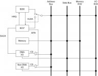
There are two different kinds of I/O devices, DMA and Non DMA devices. A DMA device will request service of the DMA controller, the non will not. The DMA controller will issue the requesting I/O device a DACK signal once it receives control of the busses. This DACK also has to block Non DMA I/O devices from responding.

8080_DMA.jpg

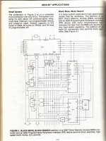
I also found an example of DMA connections in the MCS 85 manual on page A1-6. This circuit shows that the DACK signal is and-ed with the address decode of the 8255 chip (lower left corner) or other device select lines.
Although this diagram does not show any Non DMA I/O Devices, some how they needed to be prevented from responding during a DMA event. Which could be done with an inverted DACK signal. The S-100 bus doesn't have DACK signals on it, only HLDA. So, somehow, my Non DMA I/O needs to be prevented from responding when a DMA event occurs.

MCS85 DMA Example.jpg

Does this make sense?
Mike
 
That diagram harks back to the question I addressed back on a different thread of why one can't do memory-to-memory DMA on a PC XT--there's a data latch required that's not present to hold data between reading and writing. But I don't think that's what we're up against here.

In your case, this is how I see it--and I may be missing something. For your UART to go active on the bus, two conditions must be satisfied. The first is that the address must match that of the UART. The second is that an I/O Read or Write signal be present.

That second condition can be produced by the CPU or by another device if the CPU is in a hold state. That other device is the DMA controller. I think your contention is that there's an I/O read or write being asserted by the 8237 when none is explicitly being called for. This is not consistent with the 8237 operation as described in all of the datasheets that I have.

And it's this last part that I need clarification from you on.
 
Well, I think that is the nub. Does the 8237 issue a I/O R or W during a DMA transfer? I'm not an expert, but it seems to be happening on my machine. Referring to the MCS 85 manual on p 6-104, there is paragraph called "Transfer Types". It States, "each of the three active transfer modes can perform three different types of transfers. These are Read, Write and Verify. Write transfers move data from an I/O Device to memory by activating MEMW and I/OR. Read transfers move data from memory to an I/O device by activating MEMR and I/OW."
I found another example of I/O chip select in Intel Peripheral Design Handbook August 1981. Page 2-166 shows a 8088 computer with a 8237. I/O chip selects are done with a 74138 and it is gated with the AEN signal from the 8237. So the AEN blocks the chip selects to all the I/O devices, Uarts, timer and FDC (in this example). Then apparently, the DACK is used as the chip select. The I/O R & W are issued by the 8237, but not used any I/O device except the one that gets the DACK.
My diagram is wrong, a better one is.
8080_DMA.jpg
My intention is not to be difficult, I just want to better understand.
Thanks
Mike
 
The 8237 is built around read (from memory and write to IO device) or write (to memory from IO device) - it works by asserting IOR and MEMW concurrently (or IOW and MEMR concurrently) in these transfer modes. Memory-to-memory transfers are also supported I think, though not in the IBM PC for the reasons set out already.

When the 8237 has control the address bus always contains only *memory* address data; IO devices are instead selected by the DRQ/DACK lines. Hence other devices need to mask address bus matching when DMA controller has control of the system (via matching AEN).
 
Back
Top