• Please review our updated Terms and Rules here

Build your own PDP 8I, Part 3..

Hi All;

Dave, once I put it on the BreadBoard, it seems to work exactly as You have described..

"" L9 pin 5 (/PRESET) low for one clock cycle when you press the LDIR pushbutton. It should then remain high. Pin 2 (J) should remain low throughout. Pin 3 (K) should remain high until CP7 goes low - whereupon it should also go low. Pin 6 (Q) should be low until pin 5 (/PRESET) goes low - whereupon it should go high. Pin 6 (Q) should remain high until the next clock cycle after pin 3 (/K) has gone low at CP7 time - whereupon it should go low. ""

So, maybe things are not a Bad as I had previously thought and/or I mis-intrepreted what I thought I saw or it was late Saturaday Afternoon.. Or all of the above..

I am going to while I am at it put the other half of L9 with Leds for the same reason.. It will be easier for me to see, what's going on..
That's done, I was going to take a picture, but my phone/camera Battery got Low, it wasn't plugged in well enough, so it has to charge, before I can take a picture..
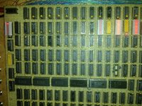
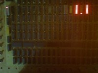
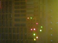
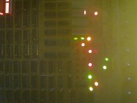
002.jpg 003.jpg 004.jpg

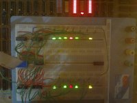
I made another change to the Board, that You can see from the pictures, I made all of the A0-9 and F0-10 signals go to Leds, instead of just what is used, this way if something changes, I don't have to guess, if it's one not connected..

"" You should be able to repeat the above tests with the manual pushbuttons LDMA, LDM, LDMB, LDPC, LDIR (already done), LDAC, EX and DEP.

The results obtained should be the same (the EXEC flip-flop should flip, you should get a series of CPx 'pulses' from 0 to 7, and the EXEC flip-flop should flip back after CP7).

Also note that during this test yo should not see any outputs from J6 (F0..F10) or J5 (A0..A10) (i.e. all of the outputs should remain at '1').

Don't forget to keep checking L10 pin 7 (it should always be '1'). ""
I have monitored L10 pin 7, with my Test Led..
And EVERYTHING Else is fine, and I tested/tried all of the Buttons..

THANK YOU Marty
 
Last edited:
By the sound of it - so far so good.

I am going to be a little busy tonight and tomorrow daytime (UK timezone) - so I will get back to you tomorrow evening with the next set of tests if that is OK with you. I have sketched out the tests on paper - I just need to convert them into electronic form.

Have a break and go back to the radio. What manufacturer and make of radio is it by the way?

Dave
 
Hi All;

Dave, Thank You for the Heads up, on Your Schedule..

"" if that is OK with you. "" Of Course..

"" Have a break and go back to the radio. What manufacturer and make of radio is it by the way? ""

I have the Radio out Now..
It is a Zenith 1940, (I think) model 587.. It belongs to a friend of mine from Church, and I hope to make it better than the condition, it came here in Electrically..
I've replaced the Electrolytic Capacitors, and now have the Paper Caps to do next, and see if that helps..
The Electrolytic Capacitors were Bad..
And eventually all of the Tubes will need to be replaced..
The 6X5 Rectifier heater was open, I think from wire shorts and possibly Bad Electrolytics..

THANK YOU Marty
 
I have a few minutes left before I turn in for the night - so I thought I would add the last couple of 'simple' tests before getting on to testing the registers out and then starting on the instructions...

Schematic LD10:

Don't forget to press STOP and CLEAR before proceeding with the tests to get the PDP-8 into a known state.

Looking at J/K flip-flop H13.

H13 pin 11 (/PRESET) should be '1'.

H13 pin 14 (J) should be '0'.

H13 pin 12 (CLK) should be clocking away.

H13 pin 13 (/K) should be '1'.

H13 pin 15 (/CLR) should be '1'.

H13 pin 11 (/PRESET) should go low for one clock cycle when you operate the LDIR pushbutton (signal SWONMANP).

H13 pin 10 (Q) should become a '1' when you operate the LDIR push-button (above).

The EXECUTE flip-flop should change state, and the clock pulses CP0 .. CP7 should be generated as a result of operating the LDIR push-button (as per the previous tests). The RUN and FETCH flip-flops should ** NOT ** change state.

H13 pin 10 (Q) should stay a '1' until H13 pin 13 (/K) changes state to a '0' at time CP7. At this point (on the next clock), H13 pin 10 (Q) should become a '0' and H13 pin 13 (/K) should revert back to a '1'.

Note that all of the outputs from L5 (instruction decoder) should become a '1' when H13 Pin 10 (Q) is a '1'.

When H13 pin 10 (Q) reverts back to a '0', one of the outputs from L5 should become active ('0'). I don't specifically care which one at this stage (this is dependent upon the random value in IR) as long as one output does go to '0'.

All activity should cease until you operate the LDIR pushbutton again whereupon the above chain of events should repeat.

Switch now to L8 (on the same schematic).

L8 pin 5 (/PRESET) should be '1'.
L8 pin 1 (/CLR) should be '1'.
L8 pin 4 (CLK) should be clocking away.
L8 pin 3 (/K) should be '1'.
L8 pin 2 (J) should be '0'.
L8 pin 6 (Q) should be '1'.

Note that operating the LDIR pushbutton should result in L8 pin 2 (J) going to a '1' at CP7 and then back to a '0'.

Not so much this time - but you will be busy tomorrow if these tests are OK!

Is this level of systematic testing helping?

Dave
 
Last edited:
Hi All;

Dave, Thank You for the Tests update..

"" Is this level of systematic testing helping? ""

VERY MUCH SO !!!!!!!

On a side Note, on Your Micro-Sequencer..
Bits 21-23 go to What lookes like another ROM, it is 3 bits input Address, and 6 bits output to ALUSEL, MBIT and /CIN..
And the Instruction Decoder is a ROM as well ??
Am I correct on these assumptions ??

I will Look at the Tests and set everything up and see what kind of results I get.. Thank You..

"" Schematic LD10:

Don't forget to press STOP and CLEAR before proceeding with the tests to get the PDP-8 into a known state.

Looking at J/K flip-flop H13.

H13 pin 11 (/PRESET) should be '1'.
Yes..
H13 pin 14 (J) should be '0'.
Yes..
H13 pin 12 (CLK) should be clocking away.
Yes..
H13 pin 13 (/K) should be '1'.
Yes..
H13 pin 15 (/CLR) should be '1'.
Yes..
H13 pin 11 (/PRESET) should go low for one clock cycle when you operate the LDIR pushbutton (signal SWONMANP).
Yes..
H13 pin 10 (Q) should become a '1' when you operate the LDIR push-button (above).
Yes..
The EXECUTE flip-flop should change state, and the clock pulses CP0 .. CP7 should be generated as a result of operating the LDIR push-button (as per the previous tests). The RUN and FETCH flip-flops should ** NOT ** change state.
Yes.. I have a Run Led, which is not changing state, currently /RUN and I don't have a FETCH Led, But, I am thinking of putting one in..
H13 pin 10 (Q) should stay a '1' until H13 pin 13 (/K) changes state to a '0' at time CP7. At this point (on the next clock), H13 pin 10 (Q) should become a '0' and H13 pin 13 (/K) should revert back to a '1'.
Yes..
Note that all of the outputs from L5 (instruction decoder) should become a '1' when H13 Pin 10 (Q) is a '1'.
Yes.. On my Instruction Decoder Led Bar..
When H13 pin 10 (Q) reverts back to a '0', one of the outputs from L5 should become active ('0'). I don't specifically care which one at this stage (this is dependent upon the random value in IR) as long as one output does go to '0'.
Yes..
All activity should cease until you operate the LDIR pushbutton again whereupon the above chain of events should repeat.

Switch now to L8 (on the same schematic).

L8 pin 5 (/PRESET) should be '1'.
L8 pin 1 (/CLR) should be '1'.
L8 pin 4 (CLK) should be clocking away.
L8 pin 3 (/K) should be '1'.
L8 pin 2 (J) should be '0'.
L8 pin 6 (Q) should be '1'.
Yes..
Note that operating the LDIR pushbutton should result in L8 pin 2 (J) going to a '1' at CP7 and then back to a '0'.
Yes..
Not so much this time - but you will be busy tomorrow if these tests are OK! ""

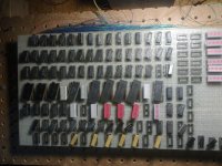
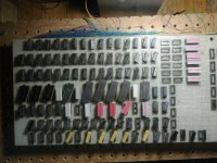
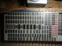
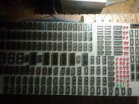
On another side Note, here is a picture of the PDP 8i Micro-coded proposed Layout.. Before I put any wire to this board..

002.jpg 003.jpg


004.jpg 001.jpg


I have already made some changes, the second picture is different from the first picture..
Please note, that some of the stuff that is in the picture is NOT what would actually be there, but is representation of what would be there..
Dave, I am sending You a Private Message..
Also, note in the not too distant future, I will have a seperate posting for this Micro-coded Board..
Dave, If You can, please take a look and see if You see anything that is glaringly missing, before I wire it up Power Wise..


THANK YOU Marty
 
Last edited:
Marty,

Things are looking better by the day with your 8I construction.

Sorry to have disappeared for a while - the trouble is that work keeps getting in the way! Unfortunately (or should that be fortunately) it pays the bills so until I retire...

The images look too compressed to be able to see any detail on the chips. Do you want to send a decent quality image to my icloud e-mail address and I will check it out.

You can create a thread called "Build your own Microcoded PDP 8I" if you wish. That's fine by me.

I think it is a good idea to permanently connect an LED to the FETCH, EXECUTE, RUN and INTERRUPT ENABLE flip-flops so we can always see the state of them. We need to make doubly sure as to which flip-flops are being activated in which order when come to debug the instructions themselves.

To move on with the next set of tests...

The next thing we need to do is to use the manual front-panel push-buttons to ensure we can load data into the internal PDP-8I registers and that we can correctly set and clear all the bits (i.e. no 'stuck' bits, bits connected to other bits etc.).

To do this, I would suggest setting up specific values on the hand-keys and loading the data into the registers. A purist would use 4096 patterns - but we can simplify that quite a bit by using a 'running '1'' or a 'running '0''.

First of all - the usual STOP and CLEAR buttons should be operated.

Next enter the following data into the hand-keys and use the LDIR push-button to load the value into the Instruction Register (IR). Check that the correct value is loaded into the IR. When the LDIR push-button is pressed, the EXECUTE flip-flop should change state (L9 pin 6 should go from a '0' to a '1') and you should get the clock pulses CP0..CP7. The EXECUTE flip-flop should change state (L9 pin 6 from '1' to '0') on the next clock pulse after CP7. Note that the RUN flip-flop (L9 pin 9) should remain at '0' and that FETCH flip-flop (L8 pin 9) should also remain at '0' throughout.

; A single '1' being shifted from right to left.
0000
0001
0002
0004
0010
0020
0040
0100
0200
0400
1000
2000
4000
0000

; A single '0' being shifted from right to left.
7777
7776
7775
7773
7767
7757
7737
7677
7577
7377
6777
5777
3777
7777

; A '1' being shifted in from the right.
0000
0001
0003
0007
0017
0037
0077
0177
0377
0777
1777
3777
7777
0000

; A '0' being shifted in from the right.
7777
7776
7774
7770
7760
7740
7700
7600
7400
7000
6000
4000
0000
7777

The patterns may look daunting - but there should be a simple repetition to them - so performing these tests shouldn't take as long as first appears.

After the LDIR (Instruction Register) has been tested, test the LDMA, LDMB, LDPC and LDAC push-buttons/registers in turn.

Don't bother about LDM, EX or DEP yet - we will get around to those later.

Let's prove the register set first.

Dave
 
Hi All;

Dave, Good to see You Back..

"" Things are looking better by the day with your 8I construction.
Only Time and Tests will tell..

Sorry to have disappeared for a while - the trouble is that work keeps getting in the way! Unfortunately (or should that be fortunately) it pays the bills so until I retire...
I UnderStand, As I am sure many others do as well..

The images look too compressed to be able to see any detail on the chips. Do you want to send a decent quality image to my icloud e-mail address and I will check it out.
OK, Thank You..

You can create a thread called "Build your own Microcoded PDP 8I" if you wish. That's fine by me.
Great, that way we can keep the two seperate.. I will make the necessary arangements..

I think it is a good idea to permanently connect an LED to the FETCH, EXECUTE, RUN and INTERRUPT ENABLE flip-flops so we can always see the state of them. We need to make doubly sure as to which flip-flops are being activated in which order when come to debug the instructions themselves.
I will add another Row of Leds just for this, there is a RUN and (I think) an Interrupt Enable, but No Fetch and No Execute..
Is E14 the Interrupt Enable Flip-flop ?? This is where I have attached it, pin 9..

001.jpg 002.jpg


In the first Picture is the /RUN Led (Red) and in the second Picture is the RUN Led (Green)..
These are four Leds, First Led is RUN, (Bi-Color) Interrupt Enable, (Green) Fetch (Orange) and Enable (Yellow)..
I will make the changes and such, and then do the Tests..

Oh, by the way, do I leave the wire connected on F1 to disable it, for the IR Register ??

THANK YOU Marty
 
Last edited:
Hi All;

Dave, Thank You for the next installment of the Tests..

"" To move on with the next set of tests...

The next thing we need to do is to use the manual front-panel push-buttons to ensure we can load data into the internal PDP-8I registers and that we can correctly set and clear all the bits (i.e. no 'stuck' bits, bits connected to other bits etc.).

To do this, I would suggest setting up specific values on the hand-keys and loading the data into the registers. A purist would use 4096 patterns - but we can simplify that quite a bit by using a 'running '1'' or a 'running '0''.

First of all - the usual STOP and CLEAR buttons should be operated.

Next enter the following data into the hand-keys and use the LDIR push-button to load the value into the Instruction Register (IR). Check that the correct value is loaded into the IR. When the LDIR push-button is pressed, the EXECUTE flip-flop should change state (L9 pin 6 should go from a '0' to a '1') and you should get the clock pulses CP0..CP7. The EXECUTE flip-flop should change state (L9 pin 6 from '1' to '0') on the next clock pulse after CP7. Note that the RUN flip-flop (L9 pin 9) should remain at '0' and that FETCH flip-flop (L8 pin 9) should also remain at '0' throughout.
YES..

Question -- When I Put something into the IR Register, via LDIR, the Data from the Switches also appears in the MB Register,
Is that Correct or Not Correct ????
Update :: When I Press any of the LDxx's the MB Register follows suite,
But when I press the LDMB it Only Loads the MB Register..
I think once we find and fix THIS problem, If there is one, then most of everything else will fall into place..

; A single '1' being shifted from right to left.
0000
0001
0002
0004
0010
0020
0040
0100
0200
0400
1000
2000
4000
0000

OK, LDAC, LDIR, LDPC, LDMB, LDM, LDMA..
; A single '0' being shifted from right to left.
7777
7776
7775
7773
7767
7757
7737
7677
7577
7377
6777
5777
3777
7777

This one is a little harder to do.. But, I figured it out, on the second set of Registers.. Now, it's not so bad..
OK, LDAC, LDIR, LDPC, LDMB, LDM, LDMA..

; A '1' being shifted in from the right.
0000
0001
0003
0007
0017
0037
0077
0177
0377
0777
1777
3777
7777
0000

OK, LDAC, LDIR, LDPC, LDMB, LDM, LDMA..
; A '0' being shifted in from the right.
7777
7776
7774
7770
7760
7740
7700
7600
7400
7000
6000
4000
0000
7777

OK, LDAC, LDIR, LDPC, LDMB, LDM, LDMA..
The patterns may look daunting - but there should be a simple repetition to them - so performing these tests shouldn't take as long as first appears.

After the LDIR (Instruction Register) has been tested, test the LDMA, LDMB, LDPC and LDAC push-buttons/registers in turn.

Don't bother about LDM, EX or DEP yet - we will get around to those later.
OK..
Let's prove the register set first. ""
OK ..

THANK YOU Marty
 
Last edited:
Marty,

It is not correct that when you store something into IR that the data also gets written into MB. You have a problem - most likely - somewhere on schematic LD15.

Try loading IR with data (not bothered what) and check the following points to see what is causing the problem (all on the MB(L) signal).

K6 pin 8 - This should always be '0'. If not, check the input pins 1,2,3,4,5,6,11 and 12. They all should be at a '1'.

K10 pin 13 - This should be at a '1' (it is the LDMB signal).

K7 pin 13 - This should be at a '1'.

E15 pin 8 - This should always be '0'. If not, check the input pins 1,2,3,4,5,6,11 and 12. They all should be at a '1'.

If all that is correct - G8 pin 9 should always be at a '0'.

Some of my reasoning: The instruction decodes feeding into K6 should be all disabled; as should the Fx signals feeding into E15. And since we are not intentionally operating the LDM, DEP or LDMB push-buttons - we shouldn't be getting activity on MB(L).

Dave
 
Last edited:
Marty,

Yes, E14 pin 9 is the interrupt enable flip-flop.

I would leave F1 disconnected from the input of E11 pin 11 on schematic LD14 (IR(L)) for now. You must remember though to tie the input of E11 that we have just disconnected from F1 'high' otherwise we will have problems with the next part of the testing!

I think that is all of your questions answered (?).

So, I guess setting the registers with all of those values was OK (from what I read) with the discrepancy that MB got loaded when it shouldn't have.

Dave
 
Hi All;

Dave, Thank You for Your Helpful Answer..

"" Some of my reasoning: The instruction decodes feeding into K6 should be all disabled; as should the Fx signals feeding into E15. And since we are not intentionally operating the LDM, DEP or LDMB push-buttons - we shouldn't be getting activity on MB(L). ""

I had thought that this was not right/correct.. Thanks for the confirmation..

"" It is not correct that when you store something in IR that the data also gets written into MB. You have a problem somewhere on schematic LD15.

Try loading IR with data (not bothered what) and check the following points to see what is causing the problem (all on the MB(L) signal).

K6 pin 8 - This should always be '0'. If not, check the input pins 1,2,3,4,5,6,11 and 12. They all should be at a '1'.
Yes..
K10 pin 13 - This should be at a '1' (it is the LDMB signal).
Yes, and it goes Low when the Switch is pushed, and then goes back to high..
K7 pin 13 - This should be at a '1'.
No, its Low (0).. I will check this out, and see If a wire is missing or not connected or not connected correctly.
It ohms out OK, But, I will do a visual on it..

I Replaced the 74LS02 and Now it Works Correctly !!!

I Re-ran the Rotating ones test on all of the LD's and all work correctly, and Do NOT show up on the MB Register..

Also, my Rant for the Day, the IC at K7 (7402), I can't Read, it is too faint, and it is a new IC.. But, Brown on Black Plastic is very Hard to Read.. I hate the new Brown on Black, and would prefer the 'old' White on Black.. But, I know the 'new' is cheaper to produce.. Just harder for a person to Read..

E15 pin 8 - This should always be '0'. If not, check the input pins 1,2,3,4,5,6,11 and 12. They all should be at a '1'.

If all that is correct - G8 pin 9 should always be at a '0'. ""

THANK YOU Marty
 
Last edited:
So - another 'bug' squashed!

Next I would like to try out the instruction decoder (L5 on schematic LD10).

Power-up and do the usual (STOP and CLEAR).

What we are going to do is to load instructions into IR (using the LDIR push-button) once again and have a look at the outputs of L5 to make sure the correct instruction is decoded.

When you depress the LDIR push-button - the FETCH and RUN flip-flops should not change state - but the EXECUTE flip-flop should and (as a result) the clock pulses CP0..CP7 should be generated. The desired value from the hand keys should be stored into IR - but the outputs from L5 should ** NOT ** be active (i.e. should all be '1') until the EXECUTE flip-flop has changed state back after CP7. At this time, one (and only one) of the outputs from L5 should be a '0'. The output should correspond to the PDP-8 instruction encoded into the top three bits (IR0..2) of IR.

Value to be stored into IR = 0000 = AND instruction = L5 pin 1 = '0'.
Value to be stored into IR = 1000 = TAD instruction = L5 pin 2 = '0'.
Value to be stored into IR = 2000 = ISZ instruction = L5 pin 3 = '0'.
Value to be stored into IR = 3000 = DCA instruction = L5 pin 4 = '0'.
Value to be stored into IR = 4000 = JMS instruction = L5 pin 5 = '0'.
Value to be stored into IR = 5000 = JMP instruction = L5 pin 6 = '0'.
Value to be stored into IR = 6000 = IOT instruction = L5 pin 7 = '0'.
Value to be stored into IR = 7000 = OPR instruction = L5 pin 9 = '0'.

If this is OK - we will have a little look at pin 4 of J7 next and then we will start on the instructions!

Dave
 
Next part of the test...

Store the identified value into IR (by use of the LDIR push-button) and monitor the state of J7 pin 4 as follows:

IR value => J7 pin 4 value.

0000 => '1' (AND DIRECT)
0400 => '1' (AND INDIRECT)
1000 => '1' (TAD DIRECT)
1400 => '1' (TAD INDIRECT)
2000 => '1' (ISZ DIRECT)
2400 => '1' (ISZ INDIRECT)
3000 => '0' (DCA DIRECT)
3400 => '1' (DCA INDIRECT)
4000 => '0' (JMS DIRECT)
4400 => '1' (JMS INDIRECT)
5000 => '0' (JMP DIRECT)
5400 => '1' (JMP INDIRECT)
6000 => '0' (IOT)
6400 => '0' (IOT)
7000 => '0' (OPR)
7400 => '0' (OPR)

Can you also double-check the following pins on J7 as well (as we will be executing our first instruction next and I want to make sure that the state machine 'should' behave itself)!

Press STOP and CLEAR first.

J7 pin 8 = '1'
J7 pin 6 = '1'
J7 pin 5 = '1'

Dave
 
Hi All;

Dave, Thank You for the Next Installment of the Tests..

On a side Note, Yesterday, before and after Your period when we can exchange Posts, I worked on the Radio and I finished replacing the rest of the Paper Caps, except for one, which I didn't have..
I ran the Radio for over 2 and one half hours last night, and it plays fine..
And that with only replacing one tube, the power rectifier with another used one..

"" Next I would like to try out the instruction decoder (L5 on schematic LD10).

Power-up and do the usual (STOP and CLEAR).

What we are going to do is to load instructions into IR (using the LDIR push-button) once again and have a look at the outputs of L5 to make sure the correct instruction is decoded.

When you depress the LDIR push-button - the FETCH and RUN flip-flops should not change state - but the EXECUTE flip-flop should and (as a result) the clock pulses CP0..CP7 should be generated. The desired value from the hand keys should be stored into IR - but the outputs from L5 should ** NOT ** be active (i.e. should all be '1') until the EXECUTE flip-flop has changed state back after CP7. At this time, one (and only one) of the outputs from L5 should be a '0'. The output should correspond to the PDP-8 instruction encoded into the top three bits (IR0..2) of IR.
YES..
Value to be stored into IR = 0000 = AND instruction = L5 pin 1 = '0'.
YES..
Value to be stored into IR = 1000 = TAD instruction = L5 pin 2 = '0'.
YES..
Value to be stored into IR = 2000 = ISZ instruction = L5 pin 3 = '0'.
YES..
Value to be stored into IR = 3000 = DCA instruction = L5 pin 4 = '0'.
YES..
Value to be stored into IR = 4000 = JMS instruction = L5 pin 5 = '0'.
YES..
Value to be stored into IR = 5000 = JMP instruction = L5 pin 6 = '0'.
YES..
Value to be stored into IR = 6000 = IOT instruction = L5 pin 7 = '0'.
YES..
Value to be stored into IR = 7000 = OPR instruction = L5 pin 9 = '0'.
YES..
If this is OK - we will have a little look at pin 4 of J7 next and then we will start on the instructions! ""

I will check L5 on the pins, as my alter one that I have connected to it in Parallel has already been working to show on the Bar Led what instruction is being called..


""" Next part of the test...

Store the identified value into IR (by use of the LDIR push-button) and monitor the state of J7 pin 4 as follows:

IR value => J7 pin 4 value.

It's Showing '0' on ALL of the Tests !!!

I am doing some checking.. Ohm wise my connections are fine..
I am going to put this on the BreadBoard.. As my Logic may be messed up..

0000 => '1' (AND DIRECT)
0400 => '1' (AND INDIRECT)
1000 => '1' (TAD DIRECT)
1400 => '1' (TAD INDIRECT)
2000 => '1' (ISZ DIRECT)
2400 => '1' (ISZ INDIRECT)
3000 => '0' (DCA DIRECT)
3400 => '1' (DCA INDIRECT)
4000 => '0' (JMS DIRECT)
4400 => '1' (JMS INDIRECT)
5000 => '0' (JMP DIRECT)
5400 => '1' (JMP INDIRECT)
6000 => '0' (IOT)
6400 => '0' (IOT)
7000 => '0' (OPR)
7400 => '0' (OPR)

Can you also double-check the following pins on J7 as well (as we will be executing our first instruction next and I want to make sure that the state machine 'should' behave itself)!

Press STOP and CLEAR first.

J7 pin 8 = '1'
J7 pin 6 = '1'
J7 pin 5 = '1'
These are Correct !!!!!

THANK YOU Marty
 
Last edited:
If J7 pin 4 is '0' all the time that is not good...

Just to make slightly more clear what I meant - J7 (SN74150) Pin 4 should go to a '1' immediately after the EXECUTE cycle has finished that loaded the value into IR.

A permanent '0' here will cause all instructions to complete their FETCH cycle (when we get to it) prematurely.

J7 pin 4 should come from the logic equation OPR + IOT + (DIRECT * (DCA + JMP + JMS))

If we load 0000 into IR (AND DIRECT) it definitely should give us a '1' at J7 pin 4.

Dave
 
Hi All;

Dave, Thanks for seeing this Now..

"" If J7 pin 4 is '0' all the time that is not good... ""

I know, which is why I am putting it on the Breadboard, with all the Leds that I need to (hopefully) find the problem..

I have since then gotten a '1' when entering 7000..

"" Just to make slightly more clear what I meant - J7 (SN74150) Pin 4 should go to a '1' immediately after the EXECUTE cycle has finished that loaded the value into IR.

A permanent '0' here will cause all instructions to complete their FETCH cycle (when we get to it) prematurely.

J7 pin 4 should come from the logic equation OPR + IOT + (DIRECT * (DCA + JMP + JMS))

If we load 0000 into IR (AND DIRECT) it definitely should give us a '1' at J7 pin 4. ""
For once I figured out what I should have and didn't have..
"" J7 pin 4 should come from the logic equation OPR + IOT + (DIRECT * (DCA + JMP + JMS)) ""

Please tell me 'What is DIRECT' Just in case I don't have it ?? I have all of the other signals from Your equations, but I am not sure about DIRECT..

So, I am looking into things..
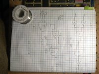
Here is a picture of my Schematic, the upper schematic is the original, the Lower is what I have wired up..


001.jpg


THANK YOU Marty
 
Last edited:
Back
Top