• Please review our updated Terms and Rules here

Build your own PDP 8I, Part 3..

Take the signal (CLK.L) from G7 pin 4 and put it to G6 pin 11 as you have said.

The signal that should now go to G7 pin 4 is not CLK.H but the INVERSE of it. Follow CLK.H back to it's source (a D-type flip-flop). Whichever port it goes to (let's say the Q output) you get the INVERSE signal for G7 pin 4 from the /Q output (or vice versa).

Just to be clear - pin 8 of G6 has nothing to do with what I am talking about. But the 7474 clock divider.

Dave
 
Hi All;

Dave, Thank You for You Answer..

I Can do that,
But, CLK.H goed thru two Inverters, as Does CLK.L .. Before it is sent out to hither and Yon..
So, do I put the Clock Invert H, thru two inverters as well ??
On the 7474 bar Q Pin 6 goes to an Inverter, which in turn goes to the Parallel Inverters for Load capability..

On the 7474 Pin 5 is Q, So Do I need to put it thru two inverter OR Can I use it as it is, It has one Inverter already on it which is used for an Led Driver.. So that would be a total of 5 Loads, would that be too much for the 7474 ??

Right now I have the Radio Out, but right After that I will try this, (straight to the 7474 pin 5) and Let You know of the Results..

Ok, I have it wired, and I cannot tell the Difference between what I had wired before and what I have wired Now.. Only future Tests will tell..

I did the Rotating 1's test and they did just fine..

During the Last few evenings and nights, I have been Re-Reading, Tracy Kidder's 'A Soul of a New Machine'..
And I keep on Hoping that very soon we will have 'La Machine'..
Dave and I have made many steps in the Right Direction, and we are not there yet, But, we are getting closer..
Each day or so, I try a short two or three line program in Memory, to see if it will Run. Which we are getting closer to after passing each section of another Test..
And we are not there yet, but, it doesn't matter, we are making progress and Having Fun all at the same time..
And one of these days to my Suprise it will work, but until then I want to keep on having Fun..
And feel the Accomplishment of Fixing it and it Passing another Test.. Thank You, Dave..

THANK YOU Marty
 
Last edited:
You're welcome. I am finding it interesting myself - although 'remote debugging' does pose its own problems. Your enthusiasm is rubbing off on me - so I am determined to get my HD6120 PDP-8/E "PDP-8 on a chip" project up and running this comming new year. So, thank you Marty as well.

As you like experimenting to get things working can I suggest attaching LED's to the following points - L10 pin 2 (schematic LD9), G6 pin 11 and G7 pin 4 (both on schematic LD14). Attach the LEDs so that ON means logical '1' and OFF means logical '0'.

Set the clock speed to very sloooow and wait until L10 pin 2 changes from '0' to '1 (LED OFF to ON). On the next transition of the 'master clock', G6 pin 11 should transition from '0' to '1' (LED OFF to ON) and then (on the next transition of the 'master clock') G7 pin 4 should transition from '0' to '1' (LED OFF to ON). At this point, L10 pin 2 should also transition from '1' to '0' (LED ON to OFF).

If this 'time sequence' is observed - the clocks are in the correct phase.

Hope this expermimental guide helps rather than the theory.

Dave
 
Hi All;

Dave, Thank You for the Encouragement and for the Next Experiment..

I think the way I have it set up is DIFFERENT than what You are currently having me do and check..
But, I will set up the Led's to make sure which one of us is correct OR if neither of us is correct.. As far as what it is doing..

"" As you like experimenting to get things working can I suggest attaching LED's to the following points - L10 pin 2 (schematic LD9), G6 pin 11 and G7 pin 4 (both on schematic LD14). Attach the LEDs so that ON means logical '1' and OFF means logical '0'.

Set the clock speed to very sloooow and wait until L10 pin 2 changes from '0' to '1 (LED OFF to ON). On the next transition of the 'master clock', G6 pin 11 should transition from '0' to '1' (LED OFF to ON) and then (on the next transition of the 'master clock') G7 pin 4 should transition from '0' to '1' (LED OFF to ON). At this point, L10 pin 2 should also transition from '1' to '0' (LED ON to OFF). ""

I think what I have now is Master Clock will turn on L10 pin 2, On the next transition of the 'master clock', G6 pin 11 should transition from '0' to '1' (LED OFF to ON) AND G7 pin 4 should transition from '1' to '0' (LED ON to OFF).
At this point, L10 pin 2 should also transition from '1' to '0' (LED ON to OFF).
But, Let me set it up for sure and I will Let You know for sure..
I might have some of the sequence wrong as far as who is on and who is off, BUT, I am sure about the second half , that is G6 pin 11 and G7 pin 4..

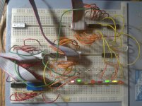
Here is Actually what I have at the present time.. !!!!!!!!!!!!!!!!!!!!

What I have now is Master Clock will turn on L10 pin 2, On the next transition of the 'master clock', G7 pin 4 transitions from '0' to '1' (LED OFF to ON) AND a moment later G6 pin 11 transitions from '1' to '0' (LED ON to OFF), But, before the Master Clock L10 pin 2 transitions from '1' to '0'..
At this point, L10 pin 2 transitions from '1' to '0' (LED ON to OFF).
001.jpg

If I UnderStand What You Want, We do Not have a three Phase Clock, we have a two Phase Clock..

"" Set the clock speed to very sloooow and wait until L10 pin 2 changes from '0' to '1 (LED OFF to ON).
Phase ONE..
On the next transition of the 'master clock', G6 pin 11 should transition from '0' to '1' (LED OFF to ON)
Phase TWO..
and then (on the next transition of the 'master clock') G7 pin 4 should transition from '0' to '1' (LED OFF to ON).
Phase THREE..
At this point, L10 pin 2 should also transition from '1' to '0' (LED ON to OFF). ""
Back to Phase ONE..

To do this We would need to ADD another half of a 7474 between the two that are Already there..
Which I could do, on the BreadBoard..

I Already have L10 and G6 and G7 out on the BreadBoard, So all I need to do is Bring out the 7474 and then I can see about making things like Your Description..

I am going to 'Fix' Phase One and Phase Three, so they match Your Description, But, for Now only on G6 pin 11 and G7 pin 4, then I will add Phase Two, so to speak..
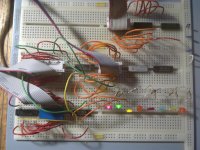

002.jpg


THANK YOU Marty
 
Last edited:
I have desscribed it as a three phase process - but it is actually a two phase clock with one of the phases inverted (to make the third phase) - so we don't need another half of a 7474.

As the latches work on the leading edge of a clock - then if you invert one of the clocks - it becomes a trailing edge in one case and a leading edge in the other (if you get my drift).

I will see if I can do a drawing if that would make it more clear.

Dave
 
Hi All;

Dave, Thanks for the Reply..

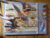
I have it WORKING as You Described, I tied G7 pin to the Existing 7474 pin 9 !!!!!!!!

I had to Put Everything to Leds for me to see it..
I put all four of the 7474 outputs to an Led..
Then it was Perfectly clear..
And I wired it up, and it worked Just fine..

003.jpg

I will be gone alot of today, I am going to a Thanksgiving Church Service, then to Pastor's for a Thanksgiving Meal..

It won't take me long to complete the change, two wires..

I am Back for a little bit, The Thanksgiving Church Service, is done, and I am waiting for Pastor's Thanksgiving Meal..

THANK YOU Marty
 
Last edited:
Yep - the complexity was me trying to explain in words how to do it and for you to turn my bumbling words into wire-wrap...

Forgot you guys have Thanksgiving today - have a happy one.

Dave
 
Hi All;

Dave, Thanks for seeing this (above)..

"" Yep - the complexity was me trying to explain in words how to do it and for you to turn my bumbling words into wire-wrap... ""

No, problem, We got it worked out..
But, The Leds solved the problem, and You saying that it wasn't a Three Phase and only a split Two phase..

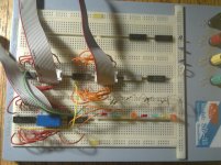
005.jpg 004.jpg

"" Forgot you guys have Thanksgiving today - have a happy one. ""

THANK YOU !!!!!!!

Now that it is Working, You can send along the Next set of Skip Tests..

It has been Running for over a half an Hour, it is doing an RAR, without the BreadBoard..
And the PC Register and the MA Register are Incrementing, while the Accumulator is Rotating..

THANK YOU Marty
 
Last edited:
Roger Marty - Over...

The SKIP instruction relies on incrementing the PC during the instruction FETCH phase and either incrementing the PC (or not) during the instruction EXECUTE phase depending upon the outcome of the test to be performed.

The instructions we will initially use are 7400 (SKIP never) and 7410 (SKIP always). Both sound pretty stupid instructions - but hang in there for a minute!

Load 7400 into the IR (using LDIR) and load 000 into PC (using LDPC) and hit CONT.

The PC should increment by 1 during the FETCH phase and not increment at all during the EXECUTE phase. This is the OPR Group 2 equivalent of the NOP instruction!

Next STOP and Load 7410 into the IR (using LDIR) and load 000 into PC (using LDPC) and hit CONT once again.

The PC should increment by 1 during the FETCH phase and also by 1 during the EXECUTE phase.

Get used to identifying where the PC gets incremented (especially learning how to identify when the PC gets incremented during the EXECUTE phase of the instruction) as you will use this visible effect to determine whether the SKIP instruction is skipping or not when you get to the next post in this series...

A little light introduction to the SKIP instruction testing after your turkey dinner...

Dave
 
Hi All;

Dave, Thank You for the Next Installment..

I have some more Cold Air Issues to take care of..

But, I will work on this In Between thru the day..
And Let You know the Results..

"" The SKIP instruction relies on incrementing the PC during the instruction FETCH phase and either incrementing the PC (or not) during the instruction EXECUTE phase depending upon the outcome of the test to be performed.

The instructions we will initially use are 7400 (SKIP never) and 7410 (SKIP always). Both sound pretty stupid instructions - but hang in there for a minute!
Actually Not, as it is a few more Tests that we can do and more thing to Pass or Fail..
Load 7400 into the IR (using LDIR) and load 000 into PC (using LDPC) and hit CONT.

The PC should increment by 1 during the FETCH phase and not increment at all during the EXECUTE phase. This is the OPR Group 2 equivalent of the NOP instruction!
YES, it Does this..
Next STOP and Load 7410 into the IR (using LDIR) and load 000 into PC (using LDPC) and hit CONT once again.

The PC should increment by 1 during the FETCH phase and also by 1 during the EXECUTE phase.
YES, This is Good as well
Get used to identifying where the PC gets incremented (especially learning how to identify when the PC gets incremented during the EXECUTE phase of the instruction) as you will use this visible effect to determine whether the SKIP instruction is skipping or not when you get to the next post in this series... ""
Remember, You asked me to Put in those Extra Leds.. One for FETCH and one for EXECUTE..

THANK YOU Marty
 
Last edited:
Excellent news.

Next part (the 'real' SKIP instructions) to follow when I get back from a bit of Christmas shopping. Cards bought...

We are now going to test out the Group 2 skips (both singly and start to look at combinations).

The 'OR' group (with IR8=0) (SMA, SZA and SNL) works by performing the logical 'OR' of the tested for conditions. Any tested for condition being met causes a SKIP.

The 'AND' group (IR8=1) (SPA, SNA and SZL) works by performing the logical 'AND' of the tested for conditions. All tested for conditions being met results in a SKIP.

What I propose first is to test out the ACCUMULATOR skip instructions followed later by the LINK skip instructions.

My table below shows the value (instruction) that should be stored into the IR, the mnemonic itself and YES or NO depending upon whether the instruction SKIPS (YES = PC incremented both during FETCH and EXECUTE) or doesn't SKIP (NO = PC incremented only during FETCH and not EXECUTE).

The values along the top of the table are the values to be loaded into the accumulator.

The procedure is STOP. Then load IR and AC with the indicated values (setting PC to 0000) and hit CONT. Look for where the PC gets incremented.

I am not sure how this table is going to turn out through (i.e. whether it is going to be readable). Let's try... Nope, the formatting turned out all wrong!


IR MNEMONIC 0000 0001 3777 4000 7777 COMMENT
7500 SMA NO NO NO YES YES Skip if minus accumulator (top bit set).
7440 SZA YES NO NO NO NO Skip if zero accumulator.
7510 SPA YES YES YES NO NO Skip if positive accumulator (i.e. not negative).
7450 SNA NO YES YES YES YES Skip if non-zero accumulator.
7540 SMA SZA YES NO NO YES YES Skip if less than or equal to zero (i.e. negative or zero).
7550 SPA SNA NO YES YES NO NO Skip if greater then zero (i.e. not negative or zero).

Next, let's test the LINK SKIP instructions.

Load 7100 (CLL) into IR and hit CONT. and then STOP. The LINK flag should be cleared.

Load 7420 (SNL) into IR and hit CONT. The instruction should not skip (i.e. PC should not be incremented during EXECUTE).

STOP.

Load 7430 into IR and hit CONT. The instruction should skip (i.e. PC should be incremented during EXECUTE).

STOP.

Load 7120 (CLL CML) into IR and hit CONT. and then STOP. The LINK flag should be set.

Load 7420 (SNL) into IR and hit CONT. The instruction should skip (i.e. PC should be incremented during EXECUTE).

STOP.

Load 7430 into IR and hit CONT. The instruction should not skip (i.e. PC should not be incremented during EXECUTE).

STOP.

You could now consider combinations of the accumulator and LINK skip instructions - but we only really want to demonstrate basic functionality. We can leave the full instruction tests to the MAINDEC suite. By the way, have you given any thought as to how you could load the MAINDEC diagnostics into your creation?

Dave
 
Last edited:
Hi All;

Dave, Thank You for the Tests, Something to do now..

"" We are now going to test out the Group 2 skips (both singly and start to look at combinations).

The 'OR' group (with IR8=0) (SMA, SZA and SNL) works by performing the logical 'OR' of the tested for conditions. Any tested for condition being met causes a SKIP.

The 'AND' group (IR8=1) (SPA, SNA and SZL) works by performing the logical 'AND' of the tested for conditions. All tested for conditions being met results in a SKIP.

What I propose first is to test out the ACCUMULATOR skip instructions followed later by the LINK skip instructions.

My table below shows the value (instruction) that should be stored into the IR, the mnemonic itself and YES or NO depending upon whether the instruction SKIPS (YES = PC incremented both during FETCH and EXECUTE) or doesn't SKIP (NO = PC incremented only during FETCH and not EXECUTE).

The values along the top of the table are the values to be loaded into the accumulator.

The procedure is STOP. Then load IR and AC with the indicated values (setting PC to 0000) and hit CONT. Look for where the PC gets incremented.

I am not sure how this table is going to turn out through (i.e. whether it is going to be readable). Let's try... Nope, the formatting turned out all wrong!
I tried it as well, and it was a No go with me to.. It looks Great in the Edit Post mode, but doesn't transfer for some reason..

I am going to do like You are doing, there will be five 'Yeses or Noes' according to whether it passes or fails..

IR MNEMONIC 0000 0001 3777 4000 7777 COMMENT
7500 SMA NO NO NO YES YES Skip if minus accumulator (top bit set).
YES, YES, YES, YES, YES..
7440 SZA YES NO NO NO NO Skip if zero accumulator.
YES, YES, YES, YES, YES..
7510 SPA YES YES YES NO NO Skip if positive accumulator (i.e. not negative).
YES, YES, YES, YES, YES..
7450 SNA NO YES YES YES YES Skip if non-zero accumulator.
YES, YES, YES, YES, YES..
7540 SMA SZA YES NO NO YES YES Skip if less than or equal to zero (i.e. negative or zero).
YES, YES, YES, YES, YES..
7550 SPA SNA NO YES YES NO NO Skip if greater then zero (i.e. not negative or zero).
YES, YES, YES, YES, YES..

TODO: Add SNL and SZL after lunch... "" OK..

"" Next, let's test the LINK SKIP instructions. OK..

Load 7100 (CLL) into IR and hit CONT. and then STOP. The LINK flag should be cleared.
YES..
Load 7420 (SNL) into IR and hit CONT. The instruction should not skip (i.e. PC should not be incremented during EXECUTE).
YES..
STOP.
OK..
Load 7430 into IR and hit CONT. The instruction should skip (i.e. PC should be incremented during EXECUTE).
YES..
STOP.
OK..
Load 7120 (CLL CML) into IR and hit CONT. and then STOP. The LINK flag should be set.
YES..
Load 7420 (SNL) into IR and hit CONT. The instruction should skip (i.e. PC should be incremented during EXECUTE).
YES..
STOP.
OK..
Load 7430 into IR and hit CONT. The instruction should not skip (i.e. PC should not be incremented during EXECUTE).
YES..
STOP.
OK..
You could now consider combinations of the accumulator and LINK skip instructions - but we only really want to demonstrate basic functionality. We can leave the full instruction tests to the MAINDEC suite. By the way, have you given any thought as to how you could load the MAINDEC diagnostics into your creation? ""

"" By the way, have you given any thought as to how you could load the MAINDEC diagnostics into your creation? ""
Not at this point, once we get everything working correctly, and able to put simple programs into Memory..
Then I will go to the Larger Memory and after making Sure that it works with a full compliment of Memory..
Then I will wire in the Serial I/O, and we can commence getting that to work, once that works then MAINDEC diagnostics can be tried..


THANK YOU Marty
 
Last edited:
Marty,

I have updated my post above with the outstanding LINK skip tests.

The post is converting multiple spaces into a single space - hence the formatting screw...

Looking at the schematics again, I think the clock signal to both halves of the E14 7474 should be wired to the same point as the accumulator clock. I think these two flip-flops could cause problems with memory and interrupt instructions due to a similar race hazard as we have found with the accumulator.

I think we can do a basic test on the JMP instruction - then we will have to start looking at the memory, Effective Address generation and then the other instructions...

Dave
 
Last edited:
Hi All;

Dave, Thanks for the Update..

"" Looking at the schematics again, I think the clock signal to both halves of the E14 7474 should be wired to the same point as the accumulator clock. I think these two flip-flops could cause problems with memory and interrupt instructions due to a similar race hazard as we have found with the accumulator. ""

When the appropiate time comes, Let's look into it..
I know that Memory seems to Work, But, we haven't gotten to that part of the Tests..
And it seems like there is a Problem between the Instruction Register and Memory.. But, since we haven't gotten to that part of the Tests, I have not mentioned it..
So, the above mentioned problem could be a part of it's (Memory and Instruction Register) problem..
But, I figure there are Other Fish in the Frying Pan at Present..

"" I think we can do a basic test on the JMP instruction - then we will have to start looking at the memory, Effective Address generation and then the other instructions... ""
Sounds like a Good Plan..

More Input !!! Everything Passes !!!

"" Looking at the schematics again, I think the clock signal to both halves of the E14 7474 should be wired to the same point as the accumulator clock. ""
There is No Accumulator Clock that I can see, it is Driven by Various CPxx's..
However, "" I think the clock signal to both halves of the E14 7474 should be wired to the same point "" as the Various Flip-flop for the other Registers.. I.e., G6 pin 11..
Am I correct in this ??

THANK YOU Marty
 
Last edited:
More - Oh alright then (just a little bit)!!!

STOP CLEAR.

Set PC to 0000
Set IR to 5042

CONT.

The PC should 'count' from 0000 to 0001 and then suddenly 'jump' to 0042 and then the PDP-8 should continuously execute the instruction 5042 (JMP 42) (i.e. the PC should should flip between 0042 and 0043).

Dead simple test - but one more thing that we know works.

The Instruction Register should have been 'disconnected' from the memory by us removing the F1 signal E11 on schematic LD14 (i.e. I am glad this 'fault' exists - as we have introduced it ourselves)!

By 'accumulate clock' what I mean is use the same clock for E14 pins 3 and 11 as we have just wired to F9, F10 and F11 pins 11 (when we get to it) - which will be next!

So yes, G6 pin 11 is another instance of this clock.

Dave
 
Hi All;

Dave, Thanks for the next set of Tests..

"" More - Oh alright then (just a little bit)!!!

STOP CLEAR.
OK..
Set PC to 0000
Set IR to 5042
OK..
CONT.
OK..
The PC should 'count' from 0000 to 0001 and then suddenly 'jump' to 0042 and then the PDP-8 should continuously execute the instruction 5042 (JMP 42) (i.e. the PC should should flip between 0042 and 0043).
YES !!!!!!!!!!
Dead simple test - but one more thing that we know works.

The Instruction Register should have been 'disconnected' from the memory by us removing the F1 signal E11 on schematic LD14 (i.e. I am glad this 'fault' exists - as we have introduced it ourselves)!
Yes, But when Testing it myself, I put F1 back in, and then changed it back for Our tests, to F1 Out.. (Tied High)..

By 'accumulate clock' what I mean is use the same clock for E14 pins 3 and 11 as we have just wired to F9, F10 and F11 pins 11 (when we get to it) - which will be next!

So yes, G6 pin 11 is another instance of this clock. ""
Good, I just got done wiring it that way..

While I am Waiting for more Tests, I am watching an Old Charlie Chan Movie, one of my Saturday morning things, quite often..

THANK YOU Marty
 
Last edited:
Ok then (things are looking mighty good so far). I am sure we will trip over a little hurdle once again shortly - but we can take that in our stride now!

Am I right in assuming that your PDP is loaded with three off 7489 devices making a grand total of 16 words of memory? I will assume it is.

We will now try the memory deposit and examine. The first set of tests should check for a data bit error and the Gray coding test for an address error.

So the usual STOP and CLEAR.

Setup MA with 0000 (first word of memory).

Deposit the first block of numbers into the memory.

; A single '1' being shifted from right to left.
0000
0001
0002
0004
0010
0020
0040
0100
0200
0400
1000
2000
4000
0000

Then re-load MA with 0000 and use the examine key to make sure that the data we have loaded is still correct and was deposited/examined to/from the right memory location. If this is OK, repeat the same procedure with the next three blocks of data to finish this test off.

; A single '0' being shifted from right to left.
7777
7776
7775
7773
7767
7757
7737
7677
7577
7377
6777
5777
3777
7777

; A '1' being shifted in from the right.
0000
0001
0003
0007
0017
0037
0077
0177
0377
0777
1777
3777
7777
0000

; A '0' being shifted in from the right.
7777
7776
7774
7770
7760
7740
7700
7600
7400
7000
6000
4000
0000
7777

If everything is OK to here - then there shouldn't be an obvious data bit error (stuck at either '1' or '0' or shorted to other data bits).

The next thing is to deposit into consecutive memory locations a Gray code as follows:

MEMORY ADDRESS => DATA VALUE

0000 => 0000
0001 => 0001
0002 => 0003
0003 => 0002
0004 => 0006
0005 => 0007
0006 => 0005
0007 => 0004
0010 => 0014
0011 => 0015
0012 => 0017
0013 => 0016
0014 => 0012
0015 => 0013
0016 => 0011
0017 => 0010

Note that there is only one data switch difference in what you enter from one memory location to the other.

Reset MA to 0000 and examine the data contents for what you have just entered.

The next test will checkout the EA address generation logic.

Dave
 
The next test is to checkout the Effective Address generation logic (EA).

We can do this by using a 'back door' in the design of this computer - and by using a PDP-8 instruction for something it was never designed for (!) Hacking at its best!

The 'back door' is that register MB is loaded with the effective address during F3 (K13 pin 3 input on schematic LD12). It is marked as 'IR' for some strange reason though on the schematic.

The instruction we are going to load into IR is an OPR Group 1 instruction - but we are not interested in anything that happens to the LINK or ACCUMULATOR registers. We are going to use the lower 7 bits of the IR as the lower 7-bits (the OFFSET) for an effective address. The upper 5 bits will be either '0' or set to the upper 5 bits of the PC register depending upon the state of IR 4.

Load 0000 into PC.
Load 7042 into IR.

CONT.

You probably need a slow clock again and need to look at register MB during F3.

The value loaded into MB during F3 should always be 0042 (but you will need to wait for the PC to count from 0000 to 7777 to make sure all combinations are checked for).

STOP.

Reload PC with 0000.

Load IR with 7242.

CONT.

The value loaded into MB during F3 should now depend upon two factors:

PPPPPOOOOOOO

Where 'P' is the corresponding bit of the PC register and 'O' is the corresponding bit of the IR register (=042).

The PC should increment by 1 during each instruction execution cycle.

This concludes the test of the EA generation logic.

Next - we are going to wire F1 back up to E11 on schematic LD14 and try some real (simple) programs. We are not going to try any more instructions than we have already tried yet - as we want to debug the instruction fetch from memory - and adding new instructions into the mix at this stage may confuse the issue.

Dave
 
Hi All;

Dave, Thank You for Hanging in there and completing the Next set of Tests..

In Your Last Post, the one above this post, I will and am going to be very Excited about what all is happening..

Ok then (things are looking mighty good so far). I am sure we will trip over a little hurdle once again shortly - but we can take that in our stride now!

Am I right in assuming that your PDP is loaded with three off 7489 devices making a grand total of 16 words of memory? I will assume it is.
Yes, That is Exactly what I have, wired In there..
We will now try the memory deposit and examine. The first set of tests should check for a data bit error and the Gray coding test for an address error.

So the usual STOP and CLEAR.

Setup MA with 0000 (first word of memory).

Deposit the first block of numbers into the memory.

; A single '1' being shifted from right to left.
0000
0001
0002
0004
0010
0020
0040
0100
0200
0400
1000
2000
4000
0000

Then re-load MA with 0000 and use the examine key to make sure that the data we have loaded is still correct and was deposited/examined to/from the right memory location. If this is OK, repeat the same procedure with the next three blocks of data to finish this test off.
YES, This is Correct..

; A single '0' being shifted from right to left.
7777
7776
7775
7773
7767
7757
7737
7677
7577
7377
6777
5777
3777
7777
YES, This is Correct as well..

; A '1' being shifted in from the right.
0000
0001
0003
0007
0017
0037
0077
0177
0377
0777
1777
3777
7777
0000
Yes, This is Working also..

; A '0' being shifted in from the right.
7777
7776
7774
7770
7760
7740
7700
7600
7400
7000
6000
4000
0000
7777
Yes, we are OK here as well..

If everything is OK to here - then there shouldn't be an obvious data bit error (stuck at either '1' or '0' or shorted to other data bits).

The next thing is to deposit into consecutive memory locations a Gray code as follows:

MEMORY ADDRESS => DATA VALUE

0000 => 0000
0001 => 0001
0002 => 0003
0003 => 0002
0004 => 0006
0005 => 0007
0006 => 0005
0007 => 0004
0010 => 0014
0011 => 0015
0012 => 0017
0013 => 0016
0014 => 0012
0015 => 0013
0016 => 0011
0017 => 0010
OK
Note that there is only one data switch difference in what you enter from one memory location to the other.

Reset MA to 0000 and examine the data contents for what you have just entered.
Yes, it checks Out !!!!
The next test will checkout the EA address generation logic. ""

I see.. I will do these tests first, Thanks for these and the Next set of Tests..


"" The next test is to checkout the Effective Address generation logic (EA).

We can do this by using a 'back door' in the design of this computer - and by using a PDP-8 instruction for something it was never designed for (!) Hacking at its best!
I LOVE it..
The 'back door' is that register MB is loaded with the effective address during F3 (K13 pin 3 input on schematic LD12). It is marked as 'IR' for some strange reason though on the schematic.

The instruction we are going to load into IR is an OPR Group 1 instruction - but we are not interested in anything that happens to the LINK or ACCUMULATOR registers. We are going to use the lower 7 bits of the IR as the lower 7-bits (the OFFSET) for an effective address. The upper 5 bits will be either '0' or set to the upper 5 bits of the PC register depending upon the state of IR 4.

Load 0000 into PC.
Load 7042 into IR.

CONT.

You probably need a slow clock again and need to look at register MB during F3.
NO, Its Loading MA at F3, NOT MB..
"" The 'back door' is that register MB is loaded with the effective address during F3 (K13 pin 3 input on schematic LD12). It is marked as 'IR' for some strange reason though on the schematic. ""
Houston, We Have a Problem !!!
Let me Look into This and Make sure I have it wired up Correctly..
"" (K13 pin 3 input on schematic LD12). "" B4..
B4 is Always High !!!!!
MA, has A3, F0, F3, F8..
MB has F5, F7, F10..

For any future people trying to follow this..
"" My Bad. It is MA that is loaded at F3 and ***NOT*** MB as I have stated.

Swap any references I have in the post above to MB with MA... ""

The value loaded into MB during F3 should always be 0042 (but you will need to wait for the PC to count from 0000 to 7777 to make sure all combinations are checked for).
YES..
STOP.
OK..
Reload PC with 0000.

Load IR with 7242.

CONT.

The value loaded into MB during F3 should now depend upon two factors:

PPPPPOOOOOOO

Where 'P' is the corresponding bit of the PC register and 'O' is the corresponding bit of the IR register (=042).

The PC should increment by 1 during each instruction execution cycle.
YES..
This concludes the test of the EA generation logic.
OK !!!
Next - we are going to wire F1 back up to E11 on schematic LD14 and try some real (simple) programs.
You Have know Idea of How Excited I currently am..
I had tried it earlier, with F1 put back in, But, I am Not going to tell You what happened..
Let's do this with No preconditions.. And Let the Games Begin..
We are not going to try any more instructions than we have already tried yet - as we want to debug the instruction fetch from memory - and adding new instructions into the mix at this stage may confuse the issue. ""

I Totally Agree..

THANK YOU Marty
 
Last edited:
Marty,

My Bad. It is MA that is loaded at F3 and ***NOT*** MB as I have stated.

Swap any references I have in the post above to MB with MA...

Dave
 
Back
Top