• Please review our updated Terms and Rules here

PDP 11/45, Part 5

Hi All;

Dave, here is a first Link, I may have a second, as well..

https://www.youtube.com/watch?v=iIsZVqhaneo

https://www.youtube.com/watch?v=Foch69Nm2F0

I have another program if You would like, it doesn't do as much though.. I will try it with Core and the SJB Board, though..

Here is my machine running one of Bill's programs, I am not sure which one.. Just for You Dave to see what it does..

https://www.youtube.com/watch?v=6ePRuwYBOGc

at '001000

'013700,
'177570,
'005300,
'001376,
'006301, (Changed this from my typing error)..
'001002,
'012701,
'000001,
'010137,
'177570,
'000765..

THANK YOU Marty
 
Last edited:
Vintagecomputer.net is Bill's site isn't it?

Here's the assembler for my test program.

Can I leave you to assemble it and try it out?

CLR R0 ; Clear R0
INC R0 ; Increment R0 (i.e. set R0 to 1)

MORE:

ROL R0 ; Rotate R0 left by 1 bit position.

MOV R0,@#177570 ; Store R0 to the "DISPLAY REGISTER"

MOV @#177570,R1 ; Pick up the state of the console switches (use them for a variable delay - 0 being the slowest).

DEL:

DEC R1 ; Subtract 1 from R1 (the delay).

BNE DEL ; Keep looping until R1 is zero (the delay has expired).

BR MORE ; Loop forever...

I think it should assemble to something like:

1000 005000 ; CLR R0
1002 005200 ; INC R0
1004 006100 ; ROL R0
1006 010037 ; MOV R0,@#177570
1010 177570 ; "
1012 013701 ; MOV @#177570,R1
1014 177570 ; "
1016 005301 ; DEC R1
1020 ??????? ; BNE to 1016 - My brain can't cope at this time of night computing relative offsets. If I tried - I would get it wrong!
1022 ??????? ; BR to 1004 - Ditto!

Dave
 
Disassembling the program in post #61 - it looks very very similar to what I have just written. The only thing I can't understand is what the instruction 006300 (ASL R0) is doing. The code has just previously cleared R0 to zero (after it has been loaded from the switch register) by repeatedly decrementing it. Performing an ASL on R0 with R0 at zero should yield zero. R0 is now zero so the next instruction (A MOV instruction) would load 1 into R1 and store R1 into the DISPLAY REGISTER. My guess would be that (with the lower console switch set to the DISPLAY REGISTER) you would get 000001 displayed (but after a delay dependent upon the setting in the switch register).

Perhaps if you changed the instruction from 006300 (ASL R0) to 006101 (ROL R1) it will do something different (i.e. display a bit of potential random rubbish rotating to the left)???

I'm off to bed... I will hopefully have a bit of time either tomorrow morning or afternoon (UK time) to catch up with your situation. I am busy in the evening though - I am installing a new monitor in our Church for our sign language interpreter to use. She is currently a bit hampered by having to look at the main projector screens for the congregation for some of her signing - so I promised to install a new monitor for her so life should be a bit easier. Just picked up all the cable I should need today so we should be 'good to go' (last words of course)!

Dave
 
Last edited:
Hi All;

Dave, Thank You for Your latest information..
No problem, Get Your Sign Language person all Happy..

I will try the corrected program as You suggested..
I Assembled Your program,
1000 005000 ; CLR R0
1002 005200 ; INC R0
1004 006100 ; ROL R0
1006 010037 ; MOV R0,@#177570
1010 177570 ; "
1012 013701 ; MOV @#177570,R1
1014 177570 ; "
1016 005301 ; DEC R1
1020 001376 ; BNE to 1016 - My brain can't cope at this time of night computing relative offsets. If I tried - I would get it wrong!
1022 000770 ; BR to 1004 - Ditto!

I MIS-Typed the '006300 Should have been '006301..
So, I will try '006301 and '006101 and see which one I like better..

I ran Your Program, Dave, and it ran fine, Until
Things warmed up and it is doing a new thing now, Not Good !!
If I (once it heats up) press Load address bit 9 goes on '001000, I then press Examine and in the Data I have '005000, I press Examine again and the Address changes to '005000 and it then goes to Address '005000.. And from there it goes into the weeds, Large Weeds..
And this is with the MOS memory, but, it does the same thing with Core.. And it is with the SJB Board..
So, Data corrupts the Address lines.. I was doing this earlier, and I let it cool off before re-running Your program..
I will try another program, just to make sure it is Not Your program, as the cause..
It's been Running Bill's chase program for quite awhile, and doesn't seem to show any problems..
I will try the other chase program..
No that chase program doesn't work for very long and it does the same type of thing, going into the Weeds as well..
I am wondering if my Register '0 is messing up or register '7..

I Finally saw Your program as it was supposed to run, after Loading in the program and setting the Loading Address bit, I put that bit back down, so nothing in the Switch Register and I Switched the Knob to DISPLAY REGISTER and then I hit Start and it ran like You meant it to run, until it went into the weeds after running awhile as it should run..
I have Changed the M8100 Data Paths Board and the M8101 GRA Board, and it is still acting up after running for a short time..
I have changed out the M8102 IRC and the M8103 RAC Boards and no change..
I don't have spares for the M8104 PDR, M8105 Trap, M8106 UBC, nor the M8116 SJb Board..

THANK YOU Marty
 
Last edited:
Hey all,

Just catching up on this thread with interest -- I just got my 11/45 past the CKBO "states" test, and will be working through the diagnostics on my KT-11 next.

Dave, re. the light chaser with the RESET in it: I believe this is supposed to work because the 11/45 microcode explicitly puts the contents of R0 on the data paths while handling the RESET instruction (see microstates RES.00, RES.10, RES.20 on FLOWS3 in the 11/45 engineering drawings.) The BR there should be jumping back just as far as the ROL. This also has the advantage the the time-delay of the RESET slows down the chase so you can see it without requiring a nested timing loop. Of course, it thrashes the heck out of the reset logic throughout the machine, though, which makes me feel a little queasy... :)

I also have a small light-chaser which uses the display register on my blog at: http://fritzm.github.io/cpu-debug-5.html. It could be shorter if I'd used the SOB instruction, and it doesn't init the light pattern for the first pass (I should revise it) but it worked at the time and it's there if anybody finds it useful.

My KT-11 seems to be basically working -- I am able to run diagnostics with it in place (disabled), and I've verified that basic relocations work when it is enabled (used this to run basic checks on all banks of my MS11-L from the front panel.) The PROG PHYS setting on the console can be quite useful for verifying relocations once Marty gets his disabled-mode working.

Let me know if you guys have any tests or measurements you'd like me make for comparison debugging as you go!

cheers,
--FritzM.

P.S. Marty re. your serial card not working in slot 26 vs. 27, you might want to check for +15V on pin CU1 in slot 26? If you recall, the +15V wiring for slots 26-28 was weird on my 11/45 backplane, and is needed for the EIA line drivers.
 
Last edited:
Dave, looking at your suggested chase program, wouldn't this go blank after it ROLs the 1 bit off into the carry? That is, won't the carry be cleared by the time it comes back around the loop for the next ROL?

(Edit: Checking the handbook I see the DEC instruction doesn't affect the carry flag, so I get it now.)
 
Last edited:
Hi All;

Fritzm, Thank You for Your Information and offer..

Please, If You have any Ideas or Suggestions Let us know..
At present You have the (that I know of) only working 11/45..
Your Program is Listed up on #61.. And Corrected from my earlier typing Mistake..
Fritzm, Could You Run Dave's program on Your machine and Let us know Your Results ?? Please..

THANK YOU Marty
 
Last edited:
Okay, I'll give it a look when I get home tonight and edit this post with the results!

(Edit: tried out Dave's program this morning and it works as expected on my 11/45.)
 
Last edited:
Hi Fritzm - welcome to the party!

I did a little bit of work on the RESET last night just before I went to bed and eventually twigged what was happening. Nice little program! Worked out the RESET instruction delays by 10 milliseconds - but the bit about R0 was new - so thanks for educating me. Interestingly, the microcode documentation states that the RESET instruction works in KERNEL mode only. Remembering back a few posts I think Marty said that with the MMU boards 'in' the SUPERVISOR lamp illuminated rather than the KERNEL lamp with the MMU boards 'out'. If this is the case, the fact that KERNEL mode wasn't selected with the MMU boards IN may account for why the program was failing - as the RESET instruction wasn't actually being executed because of the incorrect mode. Just a thought.

Anyhow, I think the fact that you have a heat-related problem Marty means that we should shelve the work on the MMU for now and concentrate on finding the little heat sensitive devil lurking in your CPU. My suggestion is to take all the boards out that you don't require (MMU - put the SJB back), Bootstrap, serial cards - basically, the bare minimum you can get away with. This will simplify what we are checking out.

You need to run one of the test programs with the rotating lamps and see when (if) it fails over a period of time. If it fails - swap ONE board for something else and try again. Keep a log of what cards you swap and the results you get. I suspect (from your previous posts) that board swapping wont solve your problem - but it repeats the tests in a controlled way and we can rule out those cards (i.e. we should know for a fact what isn't causing the problem).

As to finding the problem I need to think about that...

You appear to have a foolproof method at the moment of causing a fault to occur using the LOAD ADDRESS and EXAMINE keys. This is good - as we have something that is definitively not working as it should and we should be able to track down what is causing this symptom in a logical way.

Did I remember you saying that you had some maintenance cards? The reason I am asking is that the LOAD ADDRESS and EXAMINE keys are executed by microcode routines and we will need to single step the microcode to see which parts of the transfers are going wrong. That's my gut feeling at the moment.

My advice is - when we have found something that is wrong - don't try and fix the problem any more by board swapping. We have tried that above and it didn't work so needlessly swapping bits is futile. We need to try and work the fault through. With something that is heat sensitive this can be a long and laborious job as they are the worst problems to diagnose.

One thought whilst writing this is to put one card at a time on an extender card and use a hair dryer and a can of freezer spray. Get the test program running and then alternatively warm and cool areas of the board. If you are lucky you may be able to warm part of a card and things fail - cool that part of the board (and restart the program again) and it works until that area warms up again. We can then look to see what is around that zone of the card.

A few ideas here for you to think about...

Dave
 
Hi All;

Dave Thank You for You synopsis of the problem.. I have gotten Sick today, so things will be put on hold for awhile, until I get better.. I will be chomping at the bit until I can get back to it..

"" One thought whilst writing this is to put one card at a time on an extender card and use a hair dryer and a can of freezer spray. Get the test program running and then alternatively warm and cool areas of the board. If you are lucky you may be able to warm part of a card and things fail - cool that part of the board (and restart the program again) and it works until that area warms up again. We can then look to see what is around that zone of the card. ""

This is Exactly the method I was thinking of going.. Along with Swapping cards with a known program.. Which I have somewhat done on the first four cards..

"" Anyhow, I think the fact that you have a heat-related problem Marty means that we should shelve the work on the MMU for now and concentrate on finding the little heat sensitive devil lurking in your CPU. My suggestion is to take all the boards out that you don't require (MMU - put the SJB back), Bootstrap, serial cards - basically, the bare minimum you can get away with. This will simplify what we are checking out. ""

YES..
"' (MMU - put the SJB back), Bootstrap, serial cards, ""
I'll take out the rest and I have already swapped to the SJB Board..

"" Did I remember you saying that you had some maintenance cards? ""
YES, my own wire-wrap version..
"" The reason I am asking is that the LOAD ADDRESS and EXAMINE keys are executed by microcode routines and we will need to single step the microcode to see which parts of the transfers are going wrong. That's my gut feeling at the moment. ""

I am hoping that between You and Fritzm, we can find the correct Microcode and what Board that is on and what it is affecting and go on from there, toward finding the problem.. I still will say that the Butler had something to do with it..

"" My advice is - when we have found something that is wrong - don't try and fix the problem any more by board swapping. We have tried that above and it didn't work so needlessly swapping bits is futile. We need to try and work the fault through. With something that is heat sensitive this can be a long and laborious job as they are the worst problems to diagnose. ""

I am finding that Out..

THANK YOU Marty
 
Get well soon...

The microcode flow diagrams can be found on page 29 of 192 of the 1145 System Engineering Drawings dated June 74. The microcode states are CON.nn (console command), ADR.nn (load address command) and EXM.nn (examine command).

I have also just printed out the CPU block diagram from page 12 of the same PDF file and the microcode listings on pages 77 through 80. The numbers on the flow diagram (e.g. ADR.00 - for load address) has the number 270 in parenthesis - this refers to the word number in the microcode that this box is implemented by. The partially readable text in the box should map into the values in the microcode word which should map onto the text for which MUX path is selected etc. on the block diagram.

By single stepping each microcode word using the Marty maintenance card (I should have known you had created your own !) and using the console lamps and a logic probe (or similar) we will hopefully track down what the butler used to commit the murder and in which room!

Dave
 
+1 on the hair dryer and freeze spray suggest.

Incidentally, Marty, do you have any forced air cooling on your CPU? I don't recall seeing any from the last picture I saw of the CPU fixture you built. My 11/45 has quite a bit -- CPU cards are mounted vertically and there is a line of muffins on both the top and bottom to keep the air moving.

If you didn't already know, there are also fairly detailed descriptions of all the microcode flows in the KB11-A maint manual -- I have found these very helpful when pondering the flow diagrams in the engineering drawings.
 
Hi All;

Dave and Fritzm, Thank You for Your Helpful Suggestions..

Fritzm, "" Incidentally, Marty, do you have any forced air cooling on your CPU? I don't recall seeing any from the last picture I saw of the CPU fixture you built. My 11/45 has quite a bit -- CPU cards are mounted vertically and there is a line of muffins on both the top and bottom to keep the air moving. ""
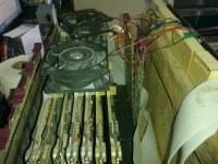
Yes, I have two fans Mounted on top of my 6 to 8 Boards, one of which I can switch on and off.. That one is a 5 volt fan, while the other one is a 12 volt fan running at 5 volts.. Hopefully, I will someday find two 6" 5 volt fans..

001.jpg

"" If you didn't already know, there are also fairly detailed descriptions of all the microcode flows in the KB11-A maint manual -- I have found these very helpful when pondering the flow diagrams in the engineering drawings. ""

YES, I have these, and that sounds like a good thing for me to do while lying in Bed, pondering my options..

Dave, "" The microcode flow diagrams can be found on page 29 of 192 of the 1145 System Engineering Drawings dated June 74. The microcode states are CON.nn (console command), ADR.nn (load address command) and EXM.nn (examine command).

I have also just printed out the CPU block diagram from page 12 of the same PDF file and the microcode listings on pages 77 through 80. The numbers on the flow diagram (e.g. ADR.00 - for load address) has the number 270 in parenthesis - this refers to the word number in the microcode that this box is implemented by. The partially readable text in the box should map into the values in the microcode word which should map onto the text for which MUX path is selected etc. on the block diagram. ""

I will take a Look at these in the Manual Description described by Fritzm..

THANK YOU Marty
 
Last edited:
Just got back from Church - good job done and it works to boot!

Sounds like a plan with the microcode...

As a starter - if you look at the actual ROM listings in the 11/45 System Engineering Drawings you will find headings like "ALU", "PCA", "AMX" and the like. These refer to tables on the two block diagrams. For example, "ALU" is a 3-bit quantity (bits [17-15] of the microcode word) and is identified on the block diagram as:

0 = NOT A
1 = B
2 = A
3 = A PLUS B
4 = NOT USED
5 = A PLUS A
6 = A MINUS B
7 = INSTRUCTION DEPENDENT

These three bits obviously refer to the function of the ALU for its two inputs (A and B) to form its output.

"AMX" identifies the MULTIPLEXER on the A input of the ALU (two bits being coded as 0 to 3):

0 = DR INPUT
1 = PCB INPUT
2 = SR INPUT
3 = BR INPUT

PCA is a single bit and is defined as 0 = NO CLOCK (don't write anything into the PCA register) 1 = LOAD (write whatever is on the ALU bus into the PCA register).

All these command signals generally occur at a certain time period.

The microcode sits at CON.00 (microcode word address 170) and CON.01 (microcode word address 167) in a loop executing the defined logic:

BA <= SR
SHFR <= DR
BR <= SWITCHES

forever until you press one of the console switches. It then branches to one of the boxes depending upon which key(s) you pressed. So (for example) pressing the "LOAD ADRS" key causes the microcode to jump from CON.01 to ADR.00 (microcode word address 270) followed by CON.20 (microcode word address 230) and then back once again to CON.00 at microcode word 170.

You can see in the ADR.00 box what action is performed at the various time pulses. These should line up with the actual microcode ROM listings.

Hope that gives you a flavour for trying to understand what is going on?

Dave
 
Hi All;

Dave, Thank You for the Explanation of the process..

I did earlier look in the KB-11 maintenance book, and saw the same type of thing..

"" Hope that gives you a flavour for trying to understand what is going on? ""

What I am going to be more concerned with is interpreting this to actual Gates on the Board, finding each MicroWord, Translating this to where it will be Implemented on the line or string of gates on say 'the PDR Board' to make something happen.. Before going to the next word in the succession and seeing where it is implemented..
I know that the various MicroWords are in one of the Boards, I am not sure which , as to of yet, which Board, whether it is the IRC or RAC or maybe GRA..
And I know I will then have to follow a certain Signal from Source ROM to the vicinity gate(s).. It's finding that signal that is turning something on or off finding it's way to where our Problem is located at..
So I sort of Understand the problem..
So, in your example above, BA <= SR
I need to find the code that does that, like 167 or 170, etc.. And go find that Multiplexer and make sure that the Bits to determine that Multiplexor is choosing the correct option namely BA.. And finding where the SR is put on the pathway, and seeing that these two happen when they are supposed to happen.. And we get a transfer, and the information is actually transferred and is correct..
I have my full page MicroCode Flow-chart that came with my machine and so it is easier for me to read..

THANK YOU Marty
 
Last edited:
Hi All;

I have found the Rom and Rom Control Listing for the Various Octal codes.. And I have found the page for the Examine switch on the UBC page..
And also the Load Address Switch, so I need to trace it back to the various MicroCode Roms and follow things through.. Good thing I have Lots of Blank paper..

THANK YOU marty
 
A few more tips for debugging microcode:

- Most of the flows have debugging "extras" that present a *lot* of extra information via the front panel when stepping with a KM11, without having to even pick up a logic probe or analyzer. On the flows, the stuff that was put in just to help with debugging is written between angle brackets ("<" and ">"). Anything that is assigned into BA will be visible on the address lights, anything put into SHFR will be visible in DATA PATHS display mode, and anything put in BR will be visible in BUS REGISTER display mode. So when you are pondering the flows, its good to ask yourself "what does the stuff in angle brackets tell me here?".

- The uADDRs display mode is your friend -- the lower seven bits show you what microstate you are in. The numeric microstate listing on page 77 of the engineering diagrams will help you quickly find the corresponding flows page when things jump through a microcode fork. Tables 6-4, 6-5, and 6-6 in the KB11-A maint manual also give a useful map of which instructions go which way through the various forks.

- Generally you can get to an instruction that seems to be malfunctioning, then drop into single microstate mode with the KM11 and step through microstates (it stops at T2 of each microstate), then when you find the microstate that is going wrong you can set up and try again but drop down into single clock step mode. Here you can see even more stuff from the front panel and generally narrow it down the specific clock phase of the specific microstate that is going awry. This gives you a very well targeted set of hardware to actually look at with the logic probe, etc. Its really wonderful how debuggable they made these machines with just the front panel and a KM11.

- A lot of console operation itself is implemented in microcode. It can get confusing stepping through console microcode vs. instruction microcode, but after you bang around in the flows for a while you get the hang of it! The display mode stuff for address, BUS REGISTER, DATA PATHS, uADDRs is pure hardware though, so that always works even when you have the clock halted etc.

- I've had a lot of trouble with the uPB microcode break stuff working reliably on my system. As a result of this, I wasted a lot of time coming to false conclusions and looking at the wrong things in the wrong places... Maybe its just my stuff and other people's CPUs or KM11s are better in this regard? For my part, I have now learned to only try using that feature as a last result.

cheers,
--FritzM.
 
Last edited:
Hi All;

Fritzm, Thank You for the much needed Information..
It will most likely make more sense to me once I start going through things and it all comes together..
I will have to determine if my unit is still working, and what switches are where, etc..

THANK YOU Marty
 
Hi All;

I have found the Rom and Rom Control Listing for the Various Octal codes.. And I have found the page for the Examine switch on the UBC page..
And also the Load Address Switch, so I need to trace it back to the various MicroCode Roms and follow things through.. Good thing I have Lots of Blank paper..

THANK YOU marty

Couple things to keep in mind. Engineers get paid to make things that are easy to build and/or design as their top priorities rather than things that are easy to debug or understand. Some processors are implemented in hardware, those are relatively easy. Others are implemented in software, like microcode, and are essentially one computer pretending to be another. That adds a layer of abstraction to the mix. But you ran into that with the PDP8 clone you were building along with the microcoded version. Remember the stuff you learned in the process. Boiled down to the basics they all "fetch and execute". Learn to think like a computer. Get out scratch paper and write down what you expect to be in each register at each step. Narrow the problem down to the simplest set of parts that fails. Build a "baby talk" program that illustrates the failure. Then drag out the tools to investigate.

Remember that:

1. What the machine is trying to do is not necessarily what you think it is trying to do.

2. If it wasn't sick you wouldn't be poking it in the guts to begin with.

3. Things learned easily are most quickly forgotten. It's the hard won knowledge that sticks with you.

Good Luck!
 
Back
Top