• Please review our updated Terms and Rules here

32K vs. 32K SRAM

Yep, I have bins and bins and bins of chips, sockets, passives, etc. So, I'm gonna use what I have. This will actually be quite similar to a RamDisk I made for my very fist S-100 TRS-80 Mod I Lev II clone I made back in the early 80's. Wish I still had the code though! I learned my lesson on throwing out old stuff....... If this works out, I can always swap the SRAMs for NVRAMs as well.....
 
Other than this, I'm also planning on using A8 to A14 from the CPU to form A0 to A7 on the RAM, so I can use INDR to transfer to/from the ram disk at block speeds. At least I think I can. I haven't actually tried it yet. But I think it should work in theory.

I was pretty confused when I read this, but finding this stackexchange article cleared it up for me… I think? Just a few observations?

  1. You said you’re going to use A8 to A14 to generate A0-A7. Aren’t you one address line short? Do you mean to use 128 byte sectors, or is this a typo?
  2. I assume the upper bits of the memory addresses are going to be stored in a latch big enough to essentially act as the LBA address for which sector you’re accessing? (I mean, you can arbitrarily break it up into ”these bits are tracks, these are sectors”, but if it’s fully populated with memory with no gaps then it is essentially LBA addressing.)
It’s an interesting idea, anyway; I guess if it works you’re getting an auto-increment address counter for free. It might not be very portable, given some Z80 systems don’t make the high addresses on the bus readily available during I/O cycles, but for your own thing, sure, why not.

The SPI memory chips Chuck mentioned would be good for a RAMDISK application like this because they usually have an auto-increment access mode built into them; just send a command and starting address down the line and subsequently read/write however many bytes you want. The only awkward part is doing efficient SPI from an old school CPU like a Z80. (All modern MCUs have hardware bitbanging facilities for that built in.)
 
A0 thru A7 (00 to FF) for the sector addressing, A8 thru A11 (0 to F) for the sectors, then A12 thru A17 for the 'tracks'. I attached my initial draft design.
 

Attachments

  • MemoryDisk.pdf
    86 KB · Views: 10
Myke, if you have an Eprom Burner and it supports GAL22V10s, consider them - I think you'll find them great for prototyping this kind of circuit :) They are very cheap from Aliexpress and you can reprogram them over and over again, trying different things.

Mostly though they really reduce the chip count dramatically. Amd they are still a simple through-hold PDIP chip.

They are pretty ancient though, and you'll need to load Windows Subsystem for Linux since all the tools for them run at command line under Linux ( older Windows executables no longer run on modern machines ).

But you could replace most of your logic gate elements with a single GAL.

Regards
David
 
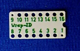
Well, I don't have an EPROM Burner, although I do have plans on how to build one; just never got around to it. Was going to burn some character generators years ago..... And I have so many parts and pieces. Heck, just yesterday I found the drawer with enough DB mounting hardware that I will never live long enough to use. And the large coffee containers I threw out years ago, chock full of chips...... This is my current stock.... Eight cabinets similar to the single one I show. what I do need is the 14 pin wire wrap socket plastic labels. I am down to only a few but they are extremely hard to find.
 

Attachments

  • 1230221250.jpg
    1230221250.jpg
    3.3 MB · Views: 5
  • 1230221250a.jpg
    1230221250a.jpg
    1.5 MB · Views: 4
FWIW, those cheap TL866 programmers available from your favorite Chinese drop-ship website support GALs.

They are pretty ancient though, and you'll need to load Windows Subsystem for Linux since all the tools for them run at command line under Linux ( older Windows executables no longer run on modern machines ).

Strictly speaking GALasm:


Also compiles fine with Cigwin; I have it installed both ways on my Win10 workstation.

I also have WinCUPL on there, but it actually lives inside a 32 bit Linux VM and runs under WINE. Yeah, it’s pretty much a loss cause to install it natively on modern Windows; it’s amazing how it’s still out there for download on the manufacturer’s website when it’s so outdated it uses Windows components that were deprecated before Windows XP came out.
 
what I do need is the 14 pin wire wrap socket plastic labels. I am down to only a few but they are extremely hard to find.
I had no idea they existed. I have considered wire wrap for a few projects, just because I love the way the wire wraps around the posts, but since I can CNC circuit boards, I tend to go the other way and work out how to make all of my PCBs single sided, no matter how complex...

Those racks remind me of my early time in a lab designing stuff in the 80s.. As a kid starting out in building z80 systems, it was like magic - a supply of every 74 series chip I could want...

It costs more for the parts for an eprom burner nowadays than it does for the burner, and while old burners don't handle GALs modern ones handle GALs and microcontrollers pretty well.

David
 
Strictly speaking GALasm:


Also compiles fine with Cigwin; I have it installed both ways on my Win10 workstation.

This is the one I use also... It lacks documentation, but works OK. Did you compile it under Windows 10 native as a CLI ? Or do you mean it works under Cigwin and Linux?

If you did build for Windows 10 native, what compiler did you use?

I get annoyed with the lack of CLI native support in Windows. I've been using FreeBASIC for a long time and the only thing I'd like to see added to it is native IP support, which isn't likely because IP and BASIC never really went together. But I am happy because all my CLI stuff, even back to QBASIC/GWBASIC can be compiled for Windows 10 :)... Not that I have any GWBASIC stuff left, it's been that long, but it still feels good that it would compile still.

Regards
David
 
Yep, 14 pin versions of these things. I have tons of 16, 20, 24, 28, and a few 40s. But the 14 pin ones are elusive.....

1675797592349.png
 
This is the one I use also... It lacks documentation, but works OK. Did you compile it under Windows 10 native as a CLI ? Or do you mean it works under Cigwin and Linux?

If you did build for Windows 10 native, what compiler did you use?

GALasm definitely had a steep learning curve, but once how GALs actually worked clicked for me I loved it. I only started messing with WinCUPL again recently because its higher-level facilities for expressing things like address calculations are kind of useful, and I also decided to suck up learning how to use its simulator function to help with some stuff I was doing with 22v10s that made use of their pin tri-stating thing. (I know you can do that in GALasm too, but I was already there for the address decoding stuff.) For simple things it's still GALasm all the way, WinCUPL is such a hassle and crashes in mighty *poof!s* in all kinds of circumstances that should just pop up error messages.

So what I did is I just compiled it with the GCC compilers available in Cygwin. Which means it isn't really truly "native", you still need to call the Cygwin wrapper if you're going to run it from a normal Windows terminal. That doesn't make it a *lot* more convenient than running it in a Linux Subsystem session, but it's "okay". That said, I kind of suspect you could probably compile it native with with the MinGW version of GCC for Windows? There's nothing really linux-centric about the code, I just haven't tried it yet? Let me know if you try it, curious if it works.

CLI support in Windows generally gives me a bad case of the sighs. I regularly find myself having to switch between Linux Subsystem, Cygwin, Git-Bash, CMD, and PowerShell
prompts, getting paths set up is a huge mess... bleah. My main hacking machine is Windows 10 Pro because I got it for free and I thought I *might* want to have the option of running commercial creativity software on it, but where I ended up I almost entirely use stuff on it that I could run with less hassle under native Linux so I guess at this point I just stick with it because it's, uhm, educational.
 
GALasm definitely had a steep learning curve, but once how GALs actually worked clicked for me I loved it.

Reading the GAL datasheet is pretty much a *must* for using GALs. I was brought up in an environment where my peers and managers were all terrified of GALs so for a while it rubbed off on me. Then I got a new job later and it focussed heavily on using GALs and on the first day, they sat me down with the GAL book and said "You have two days. Read that thoroughly and when you grok them, come back to me I'll test you."... Scary task on the first day and aside from not knowing what grok meant and having to ask, I sat down to the task. Well, the datasheet on GALs isn't two days reading. It's about 10 minutes, and if you take the time to go back through it carefully, and understand every aspect of that datasheet, it's about 2 hours max... So I went back after two hours and said "OK, I Grok them" and they got annoyed with me and said "You can't have grokked them, it's only 2 hours" and I said, "It's only 10 pages. How many times can I re-read them. All the different models are just variations on a theme."

So they tested me ( they knew I had never touched a GAL before and admitted I was fearful of them at the interview ) and sure enough, I could write the logic equations their test demanded. GALs are pretty nice like that. If you understand logic, you will understad GALs. There is a sublime beauty to the equations in GALASM.... It just clicked with me.

I think Myke would be much the same. When I see the logic he's creating, I see the same.. I get the feeling Myke would click with those equations also. And GALs are perfect for decoding addresses with lots of address lines and setting up control logic.

David
 
I think Myke would be much the same. When I see the logic he's creating, I see the same.. I get the feeling Myke would click with those equations also. And GALs are perfect for decoding addresses with lots of address lines and setting up control logic.

Yes, they are very handy for this sort of thing. I squeezed all the decoding and control logic for a board that fits the obscure keyboard-shaped Tandy 1000s (EX/HX) for:

  • decoding a conventional memory expansion from 256k to 640k
  • provides upper memory blocks with the 128K left over on the first 512K RAM chip
  • decode for a flash memory chip for BIOS extensions
  • For the above, uses a spare pin on the GAL to do something evil/abusive to the system logic via an unused DMA control line to allow memory on the card to be allocated in upper memory space reclaimed by overriding the useless DOS-in-ROM built into the 1000HX.
  • Memory/port decode/logic/chip select for 1MB of EMS memory. (The actual page frame registers are in a pair of 74LS670s)
  • I/O decode for a 16552 dual serial UART
  • All the IO decode/logic for an 8-bit XT-CF port.
Into two GAL 20v8s (one mostly on the "high" memory address lines from A19 down, the other on A9 down for the I/O decodes), with 7 input lines left over going to a DIP switch for selecting various options. (What those switches actually select evolved over time, which is another great thing about GALs; you can change your mind quite a lot without rewiring your board.) Everything else on the board is either buffers or the actual memory/peripheral chips and the whole mess fits in a space about 140x100 mm, all through-hole, two layer, with space for the hard disk header, *three* 62 pin port expansion headers, and the two 9 pin serial D-ports. If the board used discrete logic instead of the GALs it would probably be the better part of twice as large. (Which means it wouldn't fit in the computer, it'd have to be a two-board sandwich.)

They're also great for breadboarding projects because, again, you can cut sprawl immensely. It's nice to just drop one programmed GAL onto your perfboard to do some tricky custom state machine in one package instead of taking up a few rows.

Something that is useful if you're not an internal wizard with minimizing logical expressions in your head is a tool to help reduce equations to the fewest number of terms. There's an old program for Windows called "Logic Friday" that has a good tool for translating a state table into a minimized set of expressions you can pretty much lift straight into GALasm. (There are similar web toys.) Again, the main attraction of WinCUPL is it has some higher-level helpers for that sort of thing built in (in addition to address decodes it has some useful primitives for clocked entities like flip-flops and counters), but it's definitely not something you need for a project that's mostly decoding.

... That all said, I'm not really sure a GAL would save that much for Myke's design, looking at the schematic? Most of the chips in it are buffers and latches; There's a couple '138s, couple '02s, a '32, and the '74 that's acting like a latch. Making a quick count of the inputs and outputs to those parts and... I think you might *just* squeeze them all into a 22v10, but it's pretty tight. Getting rid of all those individual chip selects by using one big RAM chip would make it a sure thing, I think. ;)
 
Y'all trying real hard to pull me in the 'World of GALs'.... LOL. In looking at the logic for the GAL16V8 that the guy used in the design of the CPU board I use, I see this:

GAL16V8 ; this is the GAL type
Memory Logic 1 ; this is the signature
CLK MemReq Config A11 A12 A13 A14 A15 A1 GND ;pin declaration
/OE CSROM CSRAM0 CSRAM1 Addr0or1 Addr2or3 A2 A3 A VCC
CSROM = /MemReq + Config + A11 + A12 + A13 + A14 + A15 ;pin definitions
CSRAM0 = /A14 * /A13 * /A12 * /A11 * /Config + /MemReq + A15
CSRAM1 = /A15 + /MemReq
Addr0or1 = /A3 * /A2 * /A1
Addr2or3 = /A3 * /A2 * A1
DESCRIPTION:
This is the memory select logic for the CPUville Single board computer, with the
addition of logic to produce the Add 0 or 1 and Add 2 or 3 outputs.

So, it looks like I first have to declare the input & output signals that I need to use: WRITE, READ, IORQ, A0, A1, A2, A3, A4, A5, A6, A7, OE, WE, LA, MA, UA.... ?

Then I have to identify the logic that generates each of the outputs:
OE = /A7 * A6 * /A5 * /A4 * /A3 * A2 * /A1 * /A0 * /IORQ * /READ
WE = /A7 * A6 * /A5 * /A4 * /A3 * A2 * /A1 * /A0 * /IORQ * /WRITE
LA = /A7 * A6 * /A5 * /A4 * /A3 * A2 * /A1 * A0 * /IORQ * /WRITE
MA = /A7 * A6 * /A5 * /A4 * /A3 * A2 * A1 * /A0 * /IORQ * /WRITE
UA = /A7 * A6 * /A5 * /A4 * /A3 * A2 * A1 * A0 * /IORQ * /WRITE

Am I translating that right? I just tried to mimic what the CPU board has? If I'm sorta getting this right, then I need to figure out how the 'program' knows which pins on the actual chip get setup & programmed however.... Onward & upwards I guess....... And I guess I need to figure out how I'll program these things. I guess I can get hold of something that I can plug into a USB port and then a program to run on Win10 to burn the chip...
 
Generally WR goes straight to the WE line on the RAMs, and RD goes to the OE of the RAMs and you use CS coming out of your decoding.

Sometimes people keep CS low and then use OE as the defacto chip-select and use logic to control WE as a hack to "speed up" the access time of the rams slightly, but that's not an issue for the RAMs you're using, so using CS as a select and driving OE from RD and WE from WR would greatly simplify your design.

If so, then your GAL becomes primarily a decode only chip - eg,

CS0=/A7 * A6 * /A5 * /A4 * /A3 * A2 * /A1 * /A0 * /IORQ ; chip select 0 for I/O address 44
CS1=/A7 * A6 * /A5 * /A4 * /A3 * A2 * /A1 * A0 * /IORQ ; chip select 1 for I/O address 45

etc...

Also, you can invert the output at the line IIRC, eg;

/CS0=/A7 * A6 * /A5 * /A4 * /A3 * A2 * /A1 * /A0 * /IORQ ; chip select 0 for I/O address 44
/CS1=/A7 * A6 * /A5 * /A4 * /A3 * A2 * /A1 * A0 * /IORQ ; chip select 1 for I/O address 45

You might also use it to buffer RD and WR - since the GAL has a lot of current delivery capability for a small logic IC - eg;

OE=RD
WE=WR

Best of all, if you make a mistake, you can just reprogram the GAL. Though more commonly it gets reprogrammed because you move addresses, change functionality, add different chips for RAMs etc.

You can also design in some latched pins with a few data lines, then feed the latched output back into the logic, eg, Upper address lines. A GAL16v8 has 16 general purpose pins, of which 1 is an edge-level clock, and 8 are input/outputs. Also, you can make level triggered latches without the clock input by using feedback from the same port - eg;

LED = CS0 * /IORQ + LED * IORQ * /CS1 * /CS2 ; Latches a LED output on when CS0 is selected but goes off when CS1 or CS2 are selected by using LED as a feedback.

Or you could use the latch and latch in upper address lines to a couple of pins...

Assignment of the pins is a quirk of the software. You'll notice all the pins are listed along with whether the outputs are inverted - Well, that list is matched against the GAL type and are just a sequential list of pin assignments from pin 1 onwards - eg;

CLK MemReq Config A11 A12 A13 A14 A15 A1 GND ;pin declaration
/OE CSROM CSRAM0 CSRAM1 Addr0or1 Addr2or3 A2 A3 A VCC


This means

Pin1 CLK
Pin2 MemReq
Pin3 Config
Pin4 A11

and by the time you get to pin 10
Pin10 GND - Which if course it is, so you always see GND and VCC in the code.

The 20th term is VCC, so you can guess that Pin20 = VCC. Now all the pins are labelled.

There are some other switches in the line that tell the software whether the output is inverted and can control the OE for each output dynamically. Also, if you do it that way, you can assign almost any combination of logic as an OE for any pin - There's literally another equation line for the OE possible. This is really handy for establishing OE based on a more complicated requirement while tristating the bus outputs.

Some of the smaller GALs have some funky requirements, but the 16v8 and 22v10 are the ones I'd recommend.

David
 
Here's an idea of a GAL program I wrote. This one is a synchronous up/down counter with tri-state outputs and I/O decode... It functions as one axis of a mouse for a ZX Spectrum and decodes the bus mouse signals... Two of these, with slight variation, provides for a mouse interface with hardware decoding and 256 counts. It would be possible to also lock it so it doesn't count past overflow. It's a slightly more complex GAL program. Also, note that the higher address lines work out what the lower ones are doing. I also used another GAL to decode the buttons and debound the switches, so there's 3 gals in the design. It makes for a simple interface. Ignore the repeated comment. That was just to remind me to use .R and .E for the assembler to know that I am using the pin in register (data) mode and I'm tristating the outputs as well as driving them.

Dx is not really used here, but was reserved so that in another configuration I could either give a counter output on a bit, or other data, as I wanted to originally cover two ports with a single GAL and only needed one bit of the other port.
There's a lot you can do with a GAL. You'll also notice I use feedback extensively - so each pin maintaints it state except when it's time to change. So the registered outputs are also visible as inputs to other pins.

GAL22V10 22V10 ; 8 bit up down synchronous counter. Clock A5 A8 RD A10 IORQ A7 A6 A2 A1 A0 GND NC Dx D0 D1 D2 D6 D7 D5 D3 D4 DIR VCC D7.R = !D7 * D6 * D5 * D4 * D3 * D2 * D1 * D0 * DIR ; Y1 is a registered output => .R + D7 * !D6 * DIR + D7 * !D5 * DIR + D7 * !D4 * DIR + D7 * !D3 * DIR + D7 * !D2 * DIR + D7 * !D1 * DIR + D7 * !D0 * DIR + !D7 * !D6 * !D5 * !D4 * !D3 * !D2 * !D1 * !D0 * !DIR + D7 * D6 * !DIR + D7 * D5 * !DIR + D7 * D4 * !DIR + D7 * D3 * !DIR + D7 * D2 * !DIR + D7 * D1 * !DIR + D7 * D0 * !DIR D7.E = !IORQ * !RD * !A5 * A8 * !A10 * A6 * A7 * A0 * A1 * A2 D6.R = !D6 * D5 * D4 * D3 * D2 * D1 * D0 * DIR ; Y1 is a registered output => .R + D6 * !D5 * DIR + D6 * !D4 * DIR + D6 * !D3 * DIR + D6 * !D2 * DIR + D6 * !D1 * DIR + D6 * !D0 * DIR + !D6 * !D5 * !D4 * !D3 * !D2 * !D1 * !D0 * !DIR + D6 * D5 * !DIR + D6 * D4 * !DIR + D6 * D3 * !DIR + D6 * D2 * !DIR + D6 * D1 * !DIR + D6 * D0 * !DIR D6.E = !IORQ * !RD * !A5 * A8 * !A10 * A6 * A7 * A0 * A1 * A2 D5.R = !D5 * D4 * D3 * D2 * D1 * D0 * DIR ; Y1 is a registered output => .R + D5 * !D4 * DIR + D5 * !D3 * DIR + D5 * !D2 * DIR + D5 * !D1 * DIR + D5 * !D0 * DIR + !D5 * !D4 * !D3 * !D2 * !D1 * !D0 * !DIR + D5 * D4 * !DIR + D5 * D3 * !DIR + D5 * D2 * !DIR + D5 * D1 * !DIR + D5 * D0 * !DIR D5.E = !IORQ * !RD * !A5 * A8 * !A10 * A6 * A7 * A0 * A1 * A2 D4.R = !D4 * D3 * D2 * D1 * D0 * DIR ; Y1 is a registered output => .R + D4 * !D3 * DIR + D4 * !D2 * DIR + D4 * !D1 * DIR + D4 * !D0 * DIR + !D4 * !D3 * !D2 * !D1 * !D0 * !DIR + D4 * D3 * !DIR + D4 * D2 * !DIR + D4 * D1 * !DIR + D4 * D0 * !DIR D4.E = !IORQ * !RD * !A5 * A8 * !A10 * A6 * A7 * A0 * A1 * A2 D3.R = !D3 * D2 * D1 * D0 * DIR ; Y1 is a registered output => .R + D3 * !D2 * DIR + D3 * !D1 * DIR + D3 * !D0 * DIR + !D3 * !D2 * !D1 * !D0 * !DIR + D3 * D2 * !DIR + D3 * D1 * !DIR + D3 * D0 * !DIR D3.E = !IORQ * !RD * !A5 * A8 * !A10 * A6 * A7 * A0 * A1 * A2 D2.R = !D2 * D1 * D0 * DIR ; Y1 is a registered output => .R + D2 * !D1 * DIR + D2 * !D0 * DIR + !D2 * !D1 * !D0 * !DIR + D2 * D1 * !DIR + D2 * D0 * !DIR D2.E = !IORQ * !RD * !A5 * A8 * !A10 * A6 * A7 * A0 * A1 * A2 D1.R = !D1 * D0 * DIR ; Y1 is a registered output => .R + D1 * !D0 * DIR + !D1 * !D0 * !DIR + D1 * D0 * !DIR D1.E = !IORQ * !RD * !A5 * A8 * !A10 * A6 * A7 * A0 * A1 * A2 D0.R = !D0 ; Y1 is a registered output => .R D0.E = !IORQ * !RD * !A5 * A8 * !A10 * A6 * A7 * A0 * A1 * A2 ; rem no OE - let's see what it is since it's not connected Dx = !IORQ * !RD * !A5 * !A6 * !A7 ; DX is not really used
 
Since we're talking about example applications for GALs...

Just for laughs here's a video I made talking about the basics of GALs and describing how I use them in a homebrew video card project I'm working on:


(Note that this video covers an intermediate stage in the development of this thing, the text below describes the state as of next video about it.)

That project involves an Atmega8 MCU essentially emulating a 6545-style CRTC doing address and sync generation, and from there a pair of a GALs handle all the rest of the control and timing signal generation for the buffers, RAM/ROM chips, and output shift register. The first GAL, a 16v8, is mostly just a clock divider cutting the master clock generated by the crystal attached to the MCU into various user-selectable pixel clocks, and the second one, a 22v10, does all the dirty work counting out groups of six or eight bits (character cells can be six or eight pixels wide), controlling the chip enable/read lines for the memory chips and the buffers that alternate between the "video scan" memory fetch and the "character generation" fetch. (These buffers are not in the GAL-specific video, they were added in the next one.) It also generates a PHI clock to drive a 6502 so any memory requests from the 6502 will come on the opposite phase as requests from the video system, so it can do "no interference" sharing of memory between a CPU and video like an old 80's home computer (Apple II/Commodore 64/whatever) did.

(There's actually a third GAL in the next video where the CPU shows up, but all it does is handle the memory map selection for the 6502 tacked off on the side, it's not directly involved with video generation.)

This where GALs truly shine, making mixed-logic state machines that otherwise would require a ton of discrete parts. Both GALs have three bit counters embedded in them with logic to reset them at specific counts or generate fractional divisions. For instance, my clock divider circuit can generate an 8mhz clock from a 12mhz master clock by counting through 6 full cycles of the input clock and changing the state of the 8mhz pin four times by alternating between states that are based on both the counter register contents and the phase of the input clock signal. (The resulting output does have a 33/66% duty cycle instead of 50-50, but that's fine for this). The main control GAL also has a one-shot flip-flop embedded in it I'm kind of proud of that lets the MCU semi-asynchronously tell the GAL to actually start spitting out characters during the active period of a line and when to stop. This means the code that does address generation *only* has to count addresses in a loop, it doesn't have to twiddle a control line for every character. Certainly you could implement similar control logic with discrete chips, but... I haven't sat down and tried to actually translate everything into available TTL packages but I would guess it would be in the ballpark of at least a dozen chips, probably more.

Anyway. FWIW, I just sat down with the text editor and tried to noddle out if all the moving parts for Myke's schematic as-is would fit in a 22v10 and I think we're several pins short of being able to replace *everything*. The fact that there needs to be six output CS lines, two external buffer select lines, and swallowing up the 74LS74 requires another two registered/output pins sucks up all the outputs of a 22v10. At the very least I think there would need to be one more select output for bus buffer control. (And we're also getting really tight on inputs; there's 8 bus address lines, two data lines if the 74LS74 is internalized, IORQ, WRITE, and probably READ unless the buffer structure was modified.)

Easiest fix is probably keeping one of the 74LS138s to decode the chip select for the 6 separate RAM chips? I think that'd free up just enough to fit everything else internal. Maybe if you were lucky there would be just enough to add one more registered I/O pin and data input to give you 18 bit addressing instead of 17 bit so you could use the GAL unchanged to drive a 512K RAMdisk with single a modern SRAM on it instead.
 
Back
Top