• Please review our updated Terms and Rules here

After listening to the feedback from my previous post, I made a new design for my 80188 project.

80186 Enthusiast

Experienced Member
Joined
May 18, 2023
Messages
53
In my last post about my 80188 Prototyping Computer project, I realized I was getting way to ambitious for my project. I'd like to thank the following users who helped me see the errors of my ways:
  • Eudimorphodon (Thx for the sanity check)
  • daver2
Both of these users has given me lots of information and insight on what I should've done. I'd also like to apologize for my previous behavior, I was very over protective over my decisions I've made with that previous design and I realized how irrational all of that was. I was in way over my head with that design. With that out of the way, I'd love to show my corrected designs.
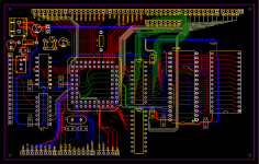
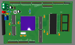
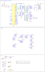
Schematic_SO8BPC_2023-06-06.pngPCB_PCB_SO8BPC_2023-06-06.pngScreenshot (129).png

No more Multi-Master Bus, No more Intel 8288 and 8289. Just a simple barebones 80188 System board with memory that also doubles as a Breakout board as all of the CPU pins are present. This design is intended to be used with a breadboard where I'll test new hardware on with some jumper cables.

as for the hardware I'll be testing with this board, Here's a small List:
  • 8279 Keyboard Controller
  • TMS9918A Video Display Processor (Before I replace it with a Raspberry Pi Pico with VGA video)
  • 8255 Peripheral Interface (PPI)
  • 8041 Universal Peripheral Interface (UPI)
That's it for this post, I'll go ahead and study x86 assembly for the 8088/80188 and create a memory map for my project.
I'll make another post that showcases what I want for the future of this project sometime soon.

Thank you for reading my post, any help and advice will be thanked and appreciated in advance!
 
Hey, we've all been there a time or two. You spent how much time and effort on the previous design. It's hard to just say "it's wrong" and move forward as your time and effort are precious to you. At least you were able to admit you were getting in a bit too deep. Some can never move from that spot.
 
Good luck with your design!
The 80186 is a bit of an odd animal. Many think that the 80286 was a later development, but in fact, the two chips were developed by different groups within Intel at the same time. The market for the 80186 was the embedded world, where, in fact, it lived for many years in everything from tape controllers and modems and printers to industrial automation. By the time you took an 80186 and added the appropriate peripheral support to make it IBM 5150 compatible, you were at a financial disadvantage. We used the 80186 as the I/O processor for an 80286 Xenix-based system.
By way of observation, I'm assuming that the peripheral chips that you've mentioned pretty much pre-date the 80186 by a fair amount. A good choice for a contemporaneous video chip, for example, might be the 82720.
 
I think you still may have a problem with your RAM chip select logic.

On a RESET, the UCS defaults to a 1KB block starting at FFC00h. This is fine, as the restart vector is in high memory. You can subsequently reprogram the UCS to whatever you want to map in the EPROM that you have.

One a RESET, the LCS and MCSn signals are disabled by default - so you have to program them anyhow.

If you use LCS, this implies the largest memory block can only(!) be 256KB.

In order to then setup the MCSn lines, you have to set your base address (for MCS0) to 40000 (as the LCS occupies the memory from 00000 to 3FFFF). I think the device enforces this?

However, once you have programmed 40000 as a base address, you are now limited to a block size of 256KB for the MCSn lines. This 256KB area is split into the four (4) MCS signals, so MCS0 is the first 64K, MCS1 is the second 64K, MCS2 is the third 64K and MCS3 is the fourth 64K. If you only have MCS0 and MCS1 used in your chip selection logic for the RAM, you are now limited to 256K + 64K + 64K = 256K + 128K = 384K.

In order to fully decode for your 512KB of RAM you either:

a) Have to include LCS and MCS0-3 into an AND gate or
b) Ignore LCS totally and use MCS0-3 into an AND gate and then set the base address to 00000 and the overall block size to 512K.

If you go for option b) you can then use a dual 4-input NAND gate and use the second gate as an inverter to give you the 4-input AND gate you require.

You can't make the MCS block size bigger (i.e. 512KB instead of 256KB), because the manual specifies that the start of the block CANNOT be 40000. The only option is 80000 and this will now overlay the UCS area for the EPROM.

Does this make sense? It may do if you read the relevant section in the manual (starting on page 6-6 of https://www.ece.unb.ca/Courses/EE3232/27216403.pdf).

I haven't checked the 'unused' input pull-ups / pull-downs yet.

Dave
Screenshot (130).png
I was thinking about using Option B from this reply from Eudimorphodon from my previous post about this project.
But now I'm considering Option A from your reply here.

Thx for the Info tho!
 
>>> Thx for the Info tho!

No problem - that's what we are here for. I am glad that you decided to 'descope' your project for the moment... I think debugging (and programming) that would have been a nightmare. You can aspire to that solution once you have cut your teeth on something that is relatively simple to get to work!

My option a) would give you the flexibility - but requires a 5-input gate...

Dave
 
I don't have a lot of bandwidth to dig in too deep to it at the moment, but this looks like a much cleaner place to start. All the peripherals you listed for the first round can probably be interfaced with this simply by using the PCSx I/O lines, and the four available IRQs should probably be sufficient so, yeah, I think it'll work.

(If you think you might be making extensive use of interrupts then there would be a case for putting the IRQ controller in the 188 into master mode and cascading at least one 8259A off it. Which, again, I don't really see a need for yet, but it's worth thinking about I guess since that decision will somewhat affect programming for things using IRQs.)

The one thing I might suggest is adding a '245 buffer on the data lines controlled by the DEN and DT/R lines; I have a vague memory of the '188's manual claiming it had stronger fan-out than an 8088/8086 in minimum mode, but it would still probably be good practice to use a buffer in front of your expansion header. (It's up to you if this buffer is also in front of the memory devices. You haven't suggested you're going to interface anything that requires DMA, which might affect that decision?)
I think you still may have a problem with your RAM chip select logic.

On a reset, the UCS defaults to a 1KB block starting at FFC00h. This is fine, as the restart vector is in high memory. You can subsequently reprogram the UCS to whatever you want to map in the EPROM that you have.

One a reset, the LCS and MCSn signals are disabled by default - so you have to program them anyhow.

If you use LCS, this implies the largest memory block can only(!) be 256KB.

In order to then setup the MCSn lines, you have to set your base address (for MCS0) to 40000 (as the LCS occupies the memory from 00000 to 3FFFF). I think the device enforces this?

However, once you have programmed 40000 as a base address, you are now limited to a block size of 256KB for the MCSn lines. This 256KB area is split into the four (4) MCS signals, so MCS0 is the first 64K, MCS1 is the second 64K, MCS2 is the third 64K and MCS3 is the fourth 64K. If you only have MCS0 and MCS1 used in your chip selection logic for the RAM, you are now limited to 256K + 64K + 64K = 256K + 128K = 384K.

Ugh. The 80186 is kind of confusing on this point, isn't it. (I missed that "base must be a multiple of the block size on a previous reading.) But I don't think all is lost here. To quote (I'm using the original 80188 manual, not the XL version) page 7-1:

With MCS3-0 prgrammed for a 512K block and either UCS or LCS programmed for a 256K block,the maximum memory area under control o f the memory chip selects is 768K.

It feels like we might have several options here:

A: Put MCS2-3 on your three input gate with LCS and don't use MCS0-1. (Don't even bring them out to a header.) MCS0-1 will activate when LCS is but if they're left hanging it won't hurt anything.

B: Use a *4* input gate for all four MCS lines and don't use LCS at all. Again, should work fine? (You'll use a 512K block size for MCS, starting at 0, each line is 128K)

C: Do the 5-input gate, use all the lines with MCS blocksize==256k

D: Decode and qualify yourself. For this you'll need to latch the S2 pin. It's not a terrible option, but I would say if you did this don't just "qualify" for the RAM chip, use the circuit you need to build for this to give you separate memory and I/O R/W signals you can use on your expansion bus. This would pretty much let you use simple 8-bit XT ISA cards unmodified if that turned out to be useful.

I feel like of all those options maybe "B" makes the most sense? ("A" requires the least modification to the design as it stands, but B: would be more "internally consistent". And... I don't know if having this capability would make sense, but in theory if you brought out LCS to a test point you could in principle do some crude bank-switching with it, maybe? IE, with an alternate ROM you could drive a completely different memory map by enabling alternate RAM on LCS and leaving the MCS lines uninitialized.)
 
Yes, I didn't read that far in the manual. Overlapping chip selects is on page 6-16 of the manual I referred to.

So, As Eudi stated, if you used LCS with a block size of 256KB and MCS with a base address of 0 and a block size of 512K you get MCS2 as the next 128KB and MCS3 as the next 128K making 256KB + 128KB + 128KB = 521KB - and all you have to do with your existing design is to reallocate MCS0 and MCS1 to be MCS2 and MCS3.

However, there are some 'quirks' that you have to be aware of when you use overlapped chip selects signals with regard to the wait states and external ready - but this is in the software not the hardware.

However, the 'quirks' don't exist if you ignore LCS and use all four MCSn lines instead.

Good idea Eudi.

Dave
 
I would still put a diode across R1 to quickly discharge the capacitor if you power cycle the machine. Again, it is not strictly necessary for a prototype.

Not sure what the purpose of U4 and the preset potentiometer are - but I see they go off-board; so I suspect you already have something in mind!

As far as I can tell, you have brought all of the pins out to the headers for future 'playing'. However, some of these will inevitably require linking to get the basic machine to run (and run reliably) without anything plugged into them.

Dave
In regards to your last point, That's where the breadboard comes in.
 
Back
Top