• Please review our updated Terms and Rules here

Apple II plus issue

I will definitely start looking at the waveforms on the ICs. I also managed to find a copy of the book Understanding the Apple II and the Apple II Reference manual. So I will start reading those as well. I think it would be safe to focus on the memory section of the computer first since it appears that it is not behaving correctly with ROM/RAM.

I am going to go ahead and still test using the II+'s power supply since it is easier to deal with than taking my IIe apart to use its power supply. Another testing idea I thought of would be to try the F8 ROM in my IIe, but am I correct in thinking that that is not possible since the IIe is quite different from the II+?

Based on what everybody has said, I highly doubt it is a problem with the keyboard circuity, but could one of the chips that handles the keyboard interface on the motherboard possibly keep triggering the ? key?
 
Another good reference is Winston Gayler's Apple II Circuit Description which is online. I wondered too about the keyboard input after the encoder. If you look in the Sam's there is a signal line labeled CLR STB which is a very narrow strobe pulse generated for each keypress which comes out of the encoder thru the ribbon. I could see it on my scope as a very narrow positive pulse. Let's say a failure on the motherboard caused that pulse line to be just a 5V logic high. It would always think a key was down and read the keyboard data repetitively. Since there was no data, all 8 bits could be high producing 11111111 which = $FF which is ?? I think. It makes sense. Is your screen all ?? or bands of another character like @@ ? Uninitialized memory is usually bands of alternate characters. If it is all ?? then it could be getting generated by bogus keyboard input w/o the keyboard connected. I would hesitate to mix ROM's between models. I don't think the reset routine would initialize properly. Maybe other's have tried this? I have a scope and a A2+ motherboard functioning out of the case for a test system so I can check waveforms against yours if needed. Another problem solved recently was a wrong TTL chip part# in a socket so verify all your chips are in the correct sockets if you think that's a possibility.
 
I just found out about the Circuit Description book while reading Understanding the Apple II. I think it will also be invaluable as well. Especially the waveform diagrams.

The screen is just a solid block of ? characters. No other characters are on the screen. And thinking about it, if the computer is thinking one key is being held down, then maybe that would explain why only the reset key combination causes the computer to respond.

I didn't even think about double checking the chips going in the correct sockets. That might be a possibility because there were some minor indications that someone may have changed a chip or two out. One had a small bit of solder on a leg (I checked that and its not shorting to anything else), and one or two chips had a pin bent so it wasn't making contact (unfortunately I can't remember specifically which two chips those were. I think it was B11, and possibly D2). I had corrected the bent pins when I was re-seating the chips. As an aside, does chip J1 (the chip nearest the power connector. I am not 100% sure of the chip's number without having the board in front of me) also have pin 1 in the same orientation as all of the other chips. I was looking through the chips yesterday and making sure they were all inserted correctly, and I noticed that that chip did not have the dot on the circuit board like all of the other ones.

Tonight when I get the chance I will take a look at the strobe signal tonight. So I wouldn't need the keyboard for testing that signal line?
 
I've found that sometimes the problem has been with the sockets becoming faulty. Those kind of issues are VERY hard to diagnose.

Tez

I have also found this in a different system (DS System 80). You can reseat the chips and it will work for a little while and inexplicably fail. The older IC sockets had poor plating plus the contact material is very thin.
 
It's been a long time since I worked on a ][ so my memory could be a little off but isn't there a 6802 that handles the keyboard I/O that you could remove to isolate everything from there to the keyboard?
 
chip J1 is same orientation as the others. if no dot on pin 1, should have a notch in the middle of the end with pin 1. chip B10 pin 11 input and pin 9 output are 0 volts with a very narrow positive 5V pulse when key pressed. Yes, without a keyboard, verify those pins are 0 volts and no pulses and definitely no DC voltage on those pins. Don't worry about small noise in the waveform. Look hard for any spikes since they occur quickly and have your scope at a slower rate where the line at least flickers. We are looking for an aberration w/o a keyboard since the problem is there. Others are suggesting bad sockets which are entirely possible. You could put pressure with your finger on each chip and wobble it to see if the problem changes or clears up.
 
It's not the keyboard circuit. If it was, you'd get a basic prompt followed by endless characters. He is not getting ROM code running right at all...
 
True, filling the screen with characters would take some time also. Maybe better off looking at waveforms around the ROM chips and select lines.
 
I was going through the chips on the board to see if each one matched the label. There was one chip that seemed suspect. The slot is labeled 74S195, but the chip in it is marked 93S00PC. I tried searching but I couldn't really find any info to see if these two numbers are equivalent. This is chip C2.

I haven't gotten the chance to start looking at the board yet, but I hope to do a little bit of analysis with the scope tonight. If I find anything interesting I will post some pictures of the traces.
 
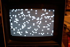
I have started looking at the board with the scope. I was going by the Sam's Computerfacts chart and I accidentally shorted out pins 3 and 4 on chip B2. The screen suddenly changed from the question mark to block like patterns and it looked like the bottom row of characters was filling up then it looked as if a carriage return was pressed. I immediately removed the probe when that happened and the pattern was still occurring. Power cycling got rid of the pattern. I also noticed that chip B1 gets quite warm during operation. I am almost thinking that that chip is bad.

Could the problem I am encountering have something to do with chips B1 and B2. Based on the references I have been consulting those chips appear to be important in the clock generation. Am I on the right track here, or am I reading the schematics wrong?
 
I found a Fairchild book online and 93S00PC has the same description as 74S195 so probably an equivalent. I just checked mine and B2 is warmer than adjacent B1 or B4 so I wouldn't be concerned. As far as the scope, if you're like me with
older eyes and glasses, it's easier to direct the scope probe from a top down aerial view. Glasses distort at angles. B1 and C2 are the majority of the timing generator which create all the clock signals off the master. I think your clocks are all running for the most part because you have character generation, the 6502 is executing instructions, etc. Just curious, when you saw the bottom row filling up and a carriage return, was there a beep on each one?
 
It's not the keyboard circuit. If it was, you'd get a basic prompt followed by endless characters. He is not getting ROM code running right at all...

I agree. But if it was as simple as pulling a 6820 to totally eliminate the keyboard (and other input) it would be nice.

If it were me, I would have shotgunned the RAM by now. Bad zero page will definitely cause this sort of problem.
 
I took a picture of the screen after pins 3 and 4 were briefly shorted on B2. The appearance of the screen slightly changes over time, and the beeping is still the same pattern that is present at start-up.

The chip that gets warm is B1, not B2. Based on my IR thermometer it reads about 90 degrees F, and the other chips read around 75 degrees F. After running for about 10 minutes or so that chip gets up to about 110 degrees F

I am going to try swapping around the ram chips some more. I have been looking at the scope traces on the RAM pins, and most of them I get a changing pattern where it will be a noisy square wave, and then another square wave that appears to be out of phase with the other one. The cycle repeats about every half second. That is on most of the pins on the right side of the chips.

I also checked chip B10 just to see. Using my scope I found that pin 9 has a DC voltage of about 4 volts, and pin 11 has a DC voltage of about 2 volts. I confirmed this with my multimeter. Just to be certain I am measuring the right chip, the chip is a 74LS74.

ScreenAfterShort.jpg
 
Your readings on B10 are definitely a problem. Confirm your pin count, etc. With keyboard connected, I have 0V on 9 and 11, both pulse high with keypress. With keyboard disconnected, I have 0V on 9 and 2V on 11 and putting my scope probe on 11
generates rapid beeps with pauses exactly like your recording !!! Pull B10 out of socket, with no keyboard and confirm beeping stops. If so, B10 is bad. As KC9UDX suggests, pulling B10 removes the input path. So do you still have an added problem after shorting pins 3 and 4 of B2 ? Or is it back to question marks onscreen? I though you said it was ok after reboot.
 
Last edited:
I removed B10, and I get a blank screen with no question marks, but the beeping continues. Later I am going to re-check to make sure I counted the pins correctly on that chip.

When I shorted pins 3 and 4 on B2 the screen stays the same after the short was removed. After reboot (power cycle) the strange screen goes away and it is back to just question marks. I haven't tried pressing the reset key to clear this, because I have been doing these checks without the keyboard attached.

I tried swapping around the RAM some more (not just swapping rows, but swapping around chips in the same row), and no luck there. I did notice that chips at the end of row D had some legs that looked black at the top. I sprayed some contact cleaner on the chip legs and tried cleaning them. I also sprayed the socket with contact cleaner to try to get a better connection. Doing that also did not result in any changes.
 
I generally replace sockets at that point. But if that's not feasible, at least take a really small screwdriver, soak the pinhole with contact clleaner, and scrape the socket until it's shiny. Do that for every pin on every suspect socket.

I generally scrape the chip pins too.
 
Right now replacing the sockets isn't feasible. I don't have any on hand. I will try to clean them the best I can, but unfortunately I don't think I have a screwdriver that is small enough.

I have been studying the schematics and the circuit description some more. I have found out that chips B6 and B7 also have to do with the keyboard circuit. If I am understanding this correctly those chips select between going to RAM or putting the keyboard data on the data bus. I found that the RAM SEL signal is on pin 15, and that appears to change over time, but when I try to check the KBD signal on pin one of those chips, it is constantly high. In the circuit description it has a line above the RAM SEL and KBD names when it references those in the text. Does that mean that those signals are inverted logic? I am thinking that maybe somehow the keyboard is constantly being read instead of the RAM and maybe junk data is being placed on the data bus.

I also did some more scouting around the board and I found another chip of the same type as B10. I swapped those two chips, and I got the constant beeping, but no question marks on the screen. I don`t know if that is significant or not. I did switch those chips back though.
 
Pin 1 of B6 and B7 (symbol = NOT KBD) originates from F13 pin 15. It is a narrow negative going pulse, easy to see on scope and is present with or w/o a keyboard connected, I measured it on mine. I don't see changes with key presses except goes high momentarily when return pressed. If pulse is missing, check F13 pin 6 for the phase0 clock signal input. You could swap F12 and F13 since they are both 74LS138
 
F13 pin 15 does not have any pulse on it. According to my scope it is just +5 volts continuous. I checked F13 pin 6, and it looks like it is getting a square wave on it. It is not the most clean signal, but it looks like it is acceptable. I also swapped F12 and F13 to see if that would do anything. It did not remedy the question mark screen, but it did eliminate the constant beeping pattern. I am going to study the circuit some more and see if there is anything else I could check. So right now could it be safe to assume that F13 might be bad?
 
Back
Top