• Please review our updated Terms and Rules here

Build your own PDP 8I, Part 2..

Hi All;

More differences between the lists..

On the INT sorted List A33 (E11) (page 34) pin 13 goes to A8-3 (G9-3) and A21-1 (E15-1) is crossed off..
On the EXT sorted List E11 (A33) (page 13) pin 13 goes to G9-3 (A8-3) and E15-1 (A21-1)..

On the INT sorted List A36 (G16) (Page 37) pin 3 goes to A43-10 (K2-10) and is crossed off and A13-5 (M15-5) is written in..
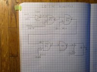
This is part of the Mod I referred to in the last posting.. A simplification of the circuit.. I have not implemented it..
On the EXT sorted List G16 (A36) (page 50) goes to K2-10 (A43-10)..

On the INT sorted List A37 (E4) (page 38) Pin 4 has it going to B19-1 (F12-1) which is crossed out and it is wired to A37-5..
Signal A0 is eliminated.. I have the pin Floating..
On the EXT sorted List E4 (A37) (Page 6) is going to F12-1 (B19-1)..

On the INT sorted List A43 (K2) (page 42) pin 8 goes to A36-4 (G16-4) and it is crossed out..
On the INT sorted List A43 (K2) (page 42) pin 9 goes to A11-2 (K4-2) and it is crossed out..
On the INT sorted List A43 (K2) (page 42) pin 10 goes to A36-3 (G16-3) and it is crossed out..
On the EXT sorted List K2 (A43) (page 72) pin 8 goes to G16-4 (A36-4)..
On the EXT sorted List K2 (A43) (page 72) pin 9 goes to K4-2 (A11-2)..
On the EXT sorted List K2 (A43) (page 72) pin 10 goes to G16-3 (A36-3)..
This finishes the Mod referred to on last posting.. I have not implemented it..

On the INT sorted List A45 (M10) (Page 44) pin 3 goes to A9-10 (M1-10) and A45-6 (M10-6) has been added..
On the INT sorted List A45 (M10) (Page 44) pin 6 goes to B47-3 (L8-3) and A10-1 (M16-1) have both been crossed out and A45-3 has been added..
A0 is eliminated and I have left M10-6 floating..
On the EXT sorted List M10 (A45) (page 106) pin 3 goes to M1-10 (A9-10)..
On the EXT sorted List M10 (A45) (page 106) pin 6 goes to L8-3 (B47-3) and M16-1 (A10-1)..

On the INT sorted List A49 (G4) (page 48) pin 2 goes to B24-12 (F2-12) and B35-4 (H8-4) Both have been crossed out and attached to P2-55 (MB4)..
On the EXT sorted List G4 (A49) (page 38) pin 2 goes to F2-12 (B24-12) and H8-4 (B35-4) (PC4)..
On this and the following Signals involving PC00 thru PC04, I have tried it using MB00 thru MB04 and it doesn't WORK !! So, I have Left all of these attached to PC00 thru PC04..

THANK YOU Marty
 
Last edited:
If single-stepping instruction 7430 (CLA CLL CML) causes the PC to be cleared, I'd say there are definitely issues. Do each of those instructions by themselves work? Do two instructions together work? That'd be where I'd begin debugging that.

Try single-stepping:
0000/ 7200 CLA
0001/ 7100 CLL
0002/ 7020 CML
0003/ 7300 CLA CLL
0004/ 7220 CLA CML
0005/ 7120 CLL CML
0006/ 7320 CLA CLL CML

Maybe you can figure out from there what the issue might be.
 
Hi All;

More differences between the lists..

On the INT sorted List A50 (G3) (page 49) pin 2 goes to B24-2 (F2-2) and B31-4 (H12-4) Both have been crossed out and attached to P1-78 (MB0)..
On the EXT sorted List G3 (A50) (page 37) pin 2 goes to F2-2 (B24-2) and H12-4 (B31-4) (PC0)..

On the INT sorted List A50 (G3) (page 49) pin 5 goes to B24-5 (F2-5) and B32-4 (H11-4) Both have been crossed out and attached to P1-84 (MB1)..
On the EXT sorted List G3 (A50) (page 37) pin 5 goes to F2-5 (B24-5) and H12-4 (B32-4) (PC1)..

On the INT sorted List A50 (G3) (page 49) pin 10 goes to B24-7 (F2-7) and (P1-89) Both have been crossed out and attached to P1-90 (MB2)..
On the EXT sorted List G3 (A50) (page 37) pin 10 goes to F2-7 (B24-7) and (P1-89) (PC2)..

On the INT sorted List A50 (G3) (page 49) pin 12 goes to B24-10 (F2-10) and B34-4 (H9-4) Both have been crossed out and attached to P1-46 (MB3)..
On the EXT sorted List G3 (A50) (page 37) pin 12 goes to F2-10 (B24-10) and H9-4 (B34-4) (PC3)..
On this and the following Signals involving PC00 thru PC04, I have tried it using MB00 thru MB04 and it doesn't WORK !! So, I have Left all of these attached to PC00 thru PC04..

Thank You Marty
 
Last edited:
Hi All;
Thank You Kyle for the information and the small program, I will probably try it tomorrow, when I get the Machine back in front of me..
At present, I am trying to get all of the Wire-Listing Differences up-loaded..
Note -- That these are Wire List differences and NOT Schematic to wire List Differences..
Schematic to wire List Differences is for another List..

THANK YOU Marty
 
Hi All;

More differences between the lists..

On the INT sorted List B19 (F12) (Page 80) pin 1 A37-4 (E4-4) is crossed from the List and B18-1 (F13-1) is left attached..
On the EXT sorted List F12 (B19) (page 30) has attached to pin 1 E4-4 (A37-4) and F13-1 (B-18-1)..
I have E4-4 floating..

On INT sorted List B24 (F2) (Page 85) pin 2 has A50-2 (G3-2) and P1-77 attached to it, A50-2 has been crossed off and B31-4 (H12-4) written in its place..
On EXT sorted List F2 (B24) (Page 20) pin 2 has G3-2 (A50-2) and P1-77 attached to it.. PC0

On INT sorted List B24 (F2) (Page 85) pin 5 has A50-5 (G3-5) and P1-83 attached to it, A50-5 has been crossed off and B32-4 (H11-4) written in its place..
On EXT sorted List F2 (B24) (Page 20) pin 5 has G3-2 (A50-5) and P1-83 attached to it.. PC1

On INT sorted List B24 (F2) (Page 85) pin 7 has A50-10 (G3-10) and B33-4 attached to it, A50-10 has been crossed off and (P1-89) written in its place..
On EXT sorted List F2 (B24) (Page 20) pin 7 has G3-10 (A50-10) and H10-4 attached to it.. PC2

On INT sorted List B24 (F2) (Page 85) pin 10 has A50-13 (G3-13) and P1-95 attached to it, A50-13 has been crossed off and B34-4 (H9-4) written in its place..
On EXT sorted List F2 (B24) (Page 20) pin 10 has G3-13 (A50-13) and P1-95 attached to it.. PC3

On INT sorted List B24 (F2) (Page 85) pin 12 has A49-2 (G4-2) and P2-56 attached to it, A49-2 has been crossed off and B35-4 (H8-4) written in its place..
On EXT sorted List F2 (B24) (Page 20) pin 12 has G4-2 (A49-2) and P2-56 attached to it.. PC4

On INT sorted List B34 (H9) (Page 92) pin 4 has A50-13 (G3-13) crossed off and B24-10 (F2-10) written in..
On the EXT sorted List H9 (B34) (page 59) pin 4 has G3-13 (A50-13) is listed..

On INT sorted List B35 (H8) (Page 93) pin 4 has A49-2 (G4-2) crossed off and B24-12 (F2-12) written in..
On the EXT sorted List H8 (B35) (page 58) pin 4 has G4-2 (A49-2) is listed..

On INT sorted List B47 (L8) (Page 105) pin 3 has C2-1 (J5-1) and A45-6 (M10-6) A45-6 is crossed off and A10-1 (M16-1) is written in..
On EXT sorted List L8 (B47) (page 93) pin 3 has J5-1 (C2-1) and M10.6 (A45-6) is listed..

That is all of the Write in Differences, I have NOT checked the rest of the IC's (Gates) that have nothing written on them..
I still need to do that..

THANK YOU Marty
 
Last edited:
Hi All;
PBirkel, Thank You for asking.. "" Which list do you think is correct(er) ""
It seems like the EXT List is more correct, and Is the one I originally Built from..

THANK YOU Marty
 
Hi All;
Kyle, here is a Simplified circuit for the PC (L) which is the signal for Loading(clocking) the PC Register..
I am only concerned with the ISZ part of the circuit, to make the ISZ work, I took G12 out of the circuit..
I had also tried switching E5 a 7400 Nand gate with a 7402 Nor gate in a different socket..
I had also tried inserting an Inverter 7404 Not gate between E6 pin 6 and G2 pin 1..
Part of what I don't understand is 'Why' the MB=0 signal is Nanded with the ISZ Signal, Yes, MB=0 would be low if there is nothing in the MB Register such as when You would have in Your program '2000' and but any other time it would be 'high' and the ISZ signal is inverted so it would be high as well.. Why is the MB=0 signal used there at all ??
I can see that They (He) had problems in this area, in the Lab manual it has
+ (ISZ . MB=0 + JMS) . CP2
in another Equation it has
+ (MB=0 * ISZ + JMS) * CP2
and an older one
+ ISZ * CP2
The period (.) I have used for the Dot in the middle of the Equation, since I don't have a dot that will be in the middle, but only the period..

002.jpg

I will get out the Machine and try Your Program, and let You know about the results..
As you probably already know, changing one circuit, can cause a change in something else..
So, I will check these again, with the modified ISZ circuit, and see if they still work..

THANK YOU Marty
 
Last edited:
Hi All;

I have a first problem,
Address 0002 Data 7020 CML does not work any more, it goes into the weeds !!
So, this is the first thing to check out..
My friend Bruce, stopped by and Helped me some, I have put the circuit back to its original wiring, and with a Re-write of my Test Program.. I probably had a mis-understanding of what the ISZ instruction was/is actually doing..
So, I am going to try this rewritten program and see if it passes, if it does, then I will retry Kyle's program from posting #22 and see if it works..
Then it would be going back to his KITT program and try to see why/where it fails..

THANK YOU Marty
 
Last edited:
Hi All;
I found a complexity of errors..
First I found that my 7404 extender cable and Pin-out board, I had made a mistake when I wired it.. The front wires were correct, pins 1 thru 7.. But, the rear wires pins 8 thru 14 were one pin off.. Also, yesterday when I had made a table of trying various combinations, Of Ic's and settings, I not only had the above mentioned mistake(s), but on one of the signals that I though I was varying, I was using the wrong pins, so I was not varying that signal at all, but some other signal..
But, after fixing all of the above it still would not work as shown in the Schematic, I found that I still had to bypass the 7404 G12 pins 1 and 2.. After tying them together on my Bread Board and not shorting out the 7404, the ISZ instruction worked, but the CLL instruction did not work..
But, by accident I got it to work.. Before that I had tied the OPG1 pin to OPG1.L instead of the OPG1.H I had retied it to when I returned everything back to the way it was in an earlier posting.. So, it was some better, and I had tried the pin that goes to the Signal F0 in one listing and F1 in the other listing, and after taking it off of the pin I had it wired to, so I could use a Jumper wire and try out each pin separately one run after the other.. I took it off of either connection, and I Ran the program, and it Ran without any problems !!
So, for now the wire is attached to nothing.. I have run the ISZ test program and it passes that.. I have run Kyles Cxx tests, (listed on post #22) and Now it Passes those as well.. I tried Kyles Kitt program, and it still fails.. I need to test RAL and RAR and SZL before trying that program again.. I also need to test the rest of the various Skip instructions..
So, that is the progress as of today/tonight..

THANK YOU Marty
 
Hi All;
RAL and RAR Fail..

Address 0000 Data 7010
Address 0001 Data 5000

I seem to have RAL and RAR fixed, I did three things, of which any of them could have solved the problem, none of which solved the problem or any one of them could have solved the problem..
When I had the board turned over, I one reconnected the wire I took off of the OPG1.L , I had been using a wire jumper.. Two, I found a strand of bare wire in the layers of wires, and removed it.. And three I wired in next to G12 a four pin connector, so I could choose between, no inverter, one inverter, or two inverters, I have it currently set for two inverters..
Next is the SZL command..

THANK YOU Marty
 
Last edited:
Hi All;
I'm on a slightly different vein, I am copying more from the Lab manual into my Notebook, I know I could just look at the file, but copying it puts it in my mind and where as reading it, would be like skimming over it.. So, I copy it for my own good..
I am then next going to see if by doing each equation that I can see, whether the results I want or need is what is showing up.. This will also help me make sure that what I have is correct.. As a for instance in one wire list signal A0 is listed and in the other it is not.. I need to determine which is correct.. Also, even though I seem to have ISZ working, it is working with a change in the circuit, and until I can prove that the change is necessary, I want to check it out..

THANK YOU Marty
 
Hi All;

M-Thompson, Thank You very much for this Link I never knew of its existence.. It's Great when someone in the know, can point to some Helpful Document or information..
I will look it over, and try to make some sense of it.. Plus, I can look over the original circuitry for the 8i and see how they did something..
On page 76 of the PDP 8i clone (Lab Manual) there is a nice description of what my machine is supposed to do.. Which I can check it against what is actually happening..

THANK YOU Marty
 
Last edited:
Marty,

Have you looked at the charts on pages 9 & 10 of the http://bitsavers.informatik.uni-stuttgart.de/pdf/dec/pdp8/pdp8i/PDP-8I_RevCY_Engineering_Drawings_Dec71.pdf prints?

If you haven't, it might give you some ideas of how the modern 8/I needs to behave.

Those charts took me back quite a few years to my days as a Computer Science student at FIU. In our mathematics & software focused course track we were exposed to Discrete Mathematics and Boolean Algebra to become (hopefully) comfortable with the kind of equations Marty has been going over. In Structured Computer Architecture we developed equations like those and then turned them into chains of gates that were a logical representation of the computer we were tasked to design. Other students who were in the hardware track took those logical gates & turned them into circuit boards that implemented the equations we had developed.

In every step we were reminded of the Computer Science version of Murphy's law, that implementation of any process or design introduces the probability of error. I bring this up to point out that the lab notes that Marty is working from very likely have errors, as will the two editions of the book. As he wires from the notes he will likely introduce more errors. It's going to be a pain in the neck to determine whether the unexplained behaviors his machine shows are the result of incorrect design, incorrect documentation of the design, or incorrect implementation of the design. As he works through the process and makes changes to the design and his notes this introduces the possibility of even more errors. I'm not throwing rocks at Marty. I think the work he's doing is amazing. It's just that there's no way he's going to avoid the side effects of working with something produced by other error prone humans, being human and error prone himself, and the backlash of the Halting Problem. Be advised that if you read the wiki at the following link your brain will likely hurt for some time. ;-)

http://en.wikipedia.org/wiki/Halting_problem

In short there is no way to mathematically prove any non trivial system is error free. Any attempt to do so (diagnostic programs and/or test fixtures) will only push the likelyhood of error back another level into the test system. The nature of the beast demands that System B created to test all possible states of System A must be more complex, and therefore more likely to have errors itself. Yet we can create tools that make the steps in the design & build process easier and expose some of the more obvious errors. One that we used years ago was a virtual breadboard that we could populate and wire in a computer to test that our logic at least implemented our equations correctly. I believe it was "LogicLab Explorer". A web search shows a number of more evolved programs, some of them free, that do what LogicLab did and more. It would probably help if someone was to run the equations that Marty is working from through such a process so he could at least have some confidence that the specs he's wiring from are correct or somewhere close to it.

I'm a rank beginner at most of this stuff, so I'll shut up now and see if some of "The Big Boys & Girls" will give us their thoughts on whether modeling the design of any or all of the LDnn designs on some appropriate test environment would get everyone to a prototype circuit board faster and/or what the best test environment might be.
 
Hi All;
First of all, Jack Thank You for Your Question.. Jack You need to go to page one (1), Posting # 9 Where PBirkel gives a Link to where He has Posted for everyone access to these Files.. Remember You need to Register to get the files..
IF you are Looking in the Book, as I have stated many times before You are Looking in the Wrong Place, the Equations are NOT the same !!

DDS, Thank You for the Long tomb of Encouragement.. I have thought and sometime either when I have time or It shows I really need to, I will put these down into TTL equivalent equations and Run them through a Simulator.. I can't think at present the name of the Language I would use, but it is a common TTL equation Language.. (VHDL) And Run it as though I was putting it into an FPGA even though I (at present) would not be actually running it in any of the FPGA Boards that I have.. I do have a Digilent (Xilinx) Spartan 3E Startup Board among others..
I have saved Your Link about the Halting problem.. Just quickly looking through it, I can tell, I won't understand most of it.. Thank You..

THANK YOU Marty
 
Last edited:
Hi All;

I have found something significant, This is only for the instructions that I have tested, as far as I know.. Such as CLA, etc, and also possibly ISZ..
I found that when I tested Kyle's Cxx program at Address '0000 it works perfectly and so does the ISZ program.. But, when I tried to run either one of them at address '0020 they failed.. WHY ??
Because some time during the first instruction, instead of updating the PC to go to the next instruction at '0021, it instead goes to '0000 !!!
So, the PC isn't getting updated, at this point I don't know the why, I just know that is what happens.. I plan on looking into it tomorrow..
I have the order of things happening for the regular instructions and now that I think about it, I have it for the ISZ instruction, So, I can look into what the Lab Manual says about the ISZ instruction, and compare what the Manual says to what I am actually getting..

THANK YOU Marty
 
Hi All;

DDS, You said that "" I'm a rank beginner at most of this stuff, "", yet from What You said at the beginning of the posting "" Those charts took me back quite a few years to my days as a Computer Science student at FIU. "" You have alot more Education and Experience than I do..
So, If You are a Rank Beginner, than what am I ?? Since I have No Education in this area..
"" In our mathematics & software focused course track we were exposed to Discrete Mathematics and Boolean Algebra to become (hopefully) comfortable with the kind of equations Marty has been going over. In Structured Computer Architecture we developed equations like those and then turned them into chains of gates that were a logical representation of the computer we were tasked to design. ""
So, You are the Kind of Person who I would Like to have here right next to me Helping me out on this.. And Guiding me through the process..
In the Lab Manual for the ISZ instruction, it states..

CLK0: MUX = MB, ALU= A+1, MB Load..
Get the old effective operand, increment it and store it in the MB register for a Memory Write..
CLK1: Issue a Write Pulse to the Memory, wait until the Memory has completed the operation..
CLK2: MUX = PC, ALU = A+1, Increment the PC..
It seems to do the same thing, no where I put the ISZ program.. I have tried it at Address '0020 and at address '0040.. Modifying thing where needed.. So that eliminates a stuck bit, or something of that sort..


THANK YOU Marty
 
Last edited:
Hi All;

DDS, You said that "" I'm a rank beginner at most of this stuff, "", yet from What You said at the beginning of the posting "" Those charts took me back quite a few years to my days as a Computer Science student at FIU. "" You have alot more Education and Experience than I do..
So, If You are a Rank Beginner, than what am I ?? Since I have No Education in this area..
"" In our mathematics & software focused course track we were exposed to Discrete Mathematics and Boolean Algebra to become (hopefully) comfortable with the kind of equations Marty has been going over. In Structured Computer Architecture we developed equations like those and then turned them into chains of gates that were a logical representation of the computer we were tasked to design. ""
So, You are the Kind of Person who I would Like to have here right next to me Helping me out on this.. And Guiding me through the process..
In the Lab Manual for the ISZ instruction, it states..

CLK0: MUX = MB, ALU= A+1, MB Load..
Get the old effective operand, increment it and store it in the MB register for a Memory Write..
CLK1: Issue a Write Pulse to the Memory, wait until the Memory has completed the operation..
CLK2: MUX = PC, ALU = A+1, Increment the PC..
It seems to do the same thing, no where I put the ISZ program.. I have tried it at Address '0020 and at address '0040.. Modifying thing where needed.. So that eliminates a stuck bit, or something of that sort..


THANK YOU Marty

I dug out my text for the Structured Computer Architecture course I mentioned and found some of my registration papers in it. One of them says all students need to certify they've had their shots by 8/29/1986. So my memories of the material are under near 30 years of other stuff in a 60+ year old brain. My suggestions may do more harm than good.

That said, the book is "Structured Computer Organization" 2nd Ed by A. S. Tanenbaum. You can get later editions as PDF's online. Chapter 4 covers the processor we built. The newer editions vary the design quite a bit. But they all have stuff like what you need. Like a block diagram. I noticed the document linked to above on a PDP8 doesn't have one. I have no idea if your notes do. But it's very helpful if you can see laid out how the buses and control leads actually handle getting an instruction from memory into the instruction register for example. You're also pretty much messed up without a schematic. If you don't have one then you should make one asap. Now for some fun stuff.

You need rock solid power. TTL doesn't like stuff like noise & ripple. You already know that from your PDP11 adventures. I put it here because others will read this and they might not know. You also need a rock solid clock. If your power isn't right and your clock isn't right it doesn't matter much what else is right, it ain't gonna work.

On my next suggestion I ran into a wall. I got a trick from a MC68k design book that I've used to good effect on other processors. The author suggested forcing the processor to execute a chain of NOP instructions in an infinite loop so he could monitor the instruction fetching, pc incrementing, and so forth. He did it a rather nifty way. He wired the equivalent bits directly onto the data bus pins at the processor. Takes all the memory and memory buss hardware right out of the picture. If your machine will run NOP's in an infinite loop for say an hour, there's a lot of stuff you've just proven good.

Keep in mind the first time I looked at a PDP8 print was today. Ditto for the PDP8 instruction set. No NOP instruction. >.<

Perhaps the PDP8 guys can suggest another way to do that.

You also have the ability to grab your processor by the nose an make it do stuff other's can't do. Like run it at an effective speed of 0 Hz. Like jam instructions directly into the IR. Look on the schematic of the PDP8 on the "Instruction Reg & Major States" page. On the middle left you see 8 gates with the inputs labeled IR0, IR1 and IR2. Those are the bits coming out of the instruction register. Those are your opcodes in hardware. You can force those 3 bits and watch how the required control signals are propagated downstream (or not).

You mentioned the timing diagrams. I'm gonna guess that those CLK0, CLK1, and CLK2 notations are what Tanenbaum calls clock subcycles. In each subcycle the clock leads are used to gate data from one location to another. The timing diagrams say what is supposed to be going where in each subcycle for each instruction. The rest is figuring out what each acronym means. I gather that EA = Effective Address, MB = Memory Bus, IR = Instruction Register. It's important that stuff happens when it's supposed to happen. Not before & not after. Gating garbage onto a bus before the outputs of the bus drivers have settled will cause disaster. That gating is what the clock is supposed to do. In the time I had to look at the PDP8 schematic I couldn't even find the clock circuitry. All of these documents were designed to be used by people who had been trained on the hardware. I'm just not a PDP8 guy and likely will never be one.

Durring my checkered career with Ma Bell I once managed a crew that maintained all 31 switches in the Miami-Dade area. One of my best #1AESS techs had never been to any formal training. But he was the kind of guy who would get out the books, put a scope on the problem and get it fixed. He was entirely self trained because he kept at a problem until he learned how it worked, what part wasn't working, and got it fixed.

Don't sell yourself short.

I have to drop this & put the hard cover back on my truck. Got to take the wife to a week long sailing school. I'll check back with this thread after that. Good Luck.
 
Back
Top