• Please review our updated Terms and Rules here

Build your own PDP 8I, Part 2..

Hi All;

I have been thinking about making some changes to this circuit, there is a fairly great amount of changes, and at present, the way I have wired up the Capacitors, that they might be shorting to the pins around them, so I am for all these reasons and a few more.. I am going to draw up the new circuit and replace all of the 14 pin sockets with 16 pin sockets and the bottom two pins will be for the Capacitor..
So, it will be like starting all over again..

:-<. But it might be a good point at which to take your "new circuit" and first verifying it by simulation before committing it to new-wires-and-sockets?
 
Hi All;

I have been thinking about making some changes to this circuit, there is a fairly great amount of changes, and at present, the way I have wired up the Capacitors, that they might be shorting to the pins around them, so I am for all these reasons and a few more.. I am going to draw up the new circuit and replace all of the 14 pin sockets with 16 pin sockets and the bottom two pins will be for the Capacitor..
So, it will be like starting all over again..

Way back in my youth, while earning my Boy Scout Woodcarving Merit Badge, I was taught the most common mistake a beginning whittler makes is taking too big a chip. In later years in Computer Science school we learned to divide a program or OS into manageable sections and debug them as separate pieces before combining them into a whole. I believe they called this "Top Down Design - Bottom Up Coding".

I hesitated to say anything before, because I didn't want to rain on your parade as you "boldly went where no man has gone before". But now that you've decided to reboot your project you might also want to rethink how you're going about it.

What I would do is break the design into subsections, then breadboard, test and debug each one before trying to put it all together. That's how the "big boys" originally did it and they had good reason to do so. Build up a generic "register" then test your ability to gate data into and out of it. Then expand that and model each of the specific PDP8 registers in the design. Do the same with the ALU. Then model the connecting busses. Test how data flows from one part to another under single step. Then build the clock and test how it does or does not control the rest of the circuit.

Smaller "chips". Smaller headaches. Localized and therefore easier to find and fix errors.

Just my $0.02 suggestion. ;-)
 
Hi All;

PBirkel, Thank You for You suggestion.. "" But it might be a good point at which to take your "new circuit" and first verifying it by simulation before committing it to new-wires-and-sockets? ""
I have for a long time tried to stay away from Simulation, because of the steep Learning Curve of getting it into my head and the computer..
As well as all of the typing and debugging of that just to get it right, for the Schematic.. I could be all Wrong, but it seemed easier to just wire it, than all that would be needed to get it done by getting it into simulation..
I have looked at what everyone has offered earlier, and I would need to figure out, exactly how to enter it in IC mode instead of gate mode, which I never got past..

DDS, Thank You for the reply and the suggestion, Actually, I have been kind of doing this already..
As the Schematic is divided into sections, that are parts of the whole thing, and I have been checking each section..
But, I can in some cases further divide the sections into smaller parts..
And since they are machine wire wrap sockets, I could only put in the Ic's that are needed for a particular circuit..
I can and did put a circuit or two on my Breadboard and made what didn't work, work.. Trying different things, until I proved it would work as the origional circuit was, or what was needed to make it work..
Mostly, the 'fixes' are having to do with Ic counts, in other words on the Alu there are five signals that control what the Alu does, and in each of these there are anywhere from three to maybe eight gate delays on any of the control signals, and so they all don't reach the Alu at the same time..
Most of these are things like having a 7402 followed by a 7404, which I can instead replace with a 7432, and eliminate the 7404.. Or a 7400 followed by a 7404, which I can replace by a 7408 and eliminate the 7404..
And so by doing this I can bring them all closer to the three gates of delay..
Also, I can replace the 74175 which is a 6 register part, so two are required, with a 74174, which has 4 registers per part, so it will require three of these for the 12 bits.. But by doing this I can in a number of places eliminate 12 (7404) inversion gates and have less loading on the 74174, than was on the 74175..

THANK YOU Marty
 
Last edited:
"Mostly, the 'fixes' are having to do with Ic counts, in other words on the Alu there are five signals that control what the Alu does, and in each of these there are anywhere from three to maybe eight gate delays on any of the control signals, and so they all don't reach the Alu at the same time.."

Seems like you're looking at two main possibilities. In all of the systems I've worked with gate delays were mostly made irrelevant by either the processor clock's gating of data and signal flows or by delay lines. Here I should point out that I've never worked with a PDP8. Things were sometimes done differently back at the dawn of time. Machines spoke in inscrutable tongues like FIELDATA and EBCDIC. But IMHO your ALU should be inhibited by the clock from doing anything with its inputs until such a time as all the inputs should be ready. If that's not happening you likely have a problem with the clock control of the ALU. IF the ALU is waiting until the correct time and one or more of your inputs are not yet ready, then you likely have a problem with whatever is supposed to be propagating that signal.

The key to debugging this would be the processor timing diagrams for the design you're building. Hopefully you have them, can make them, or can get them from somebody on here who can. You might be able to use the diagrams for the PDP8 that your clone is trying to mimic if your clone is close enough to the original hardware wise. Then it will be a matter of dragging out the scope or logic analyzer of your choice and nailing it down.
 
Hi All;

DDS, Thank You for Your answer, and suggestions..

""
Seems like you're looking at two main possibilities. In all of the systems I've worked with gate delays were mostly made irrelevant by either the processor clock's gating of data and signal flows or by delay lines. ""
I think that this is mostly true, but, I can't say in this case..
"" Here I should point out that I've never worked with a PDP8. Things were sometimes done differently back at the dawn of time. Machines spoke in inscrutable tongues like FIELDATA and EBCDIC.
""But IMHO your ALU should be inhibited by the clock from doing anything with its inputs until such a time as all the inputs should be ready. ""
I can't say that it has this..
"" If that's not happening you likely have a problem with the clock control of the ALU. IF the ALU is waiting until the correct time and one or more of your inputs are not yet ready, then you likely have a problem with whatever is supposed to be propagating that signal. ""
That is what I hope to fix, this time around..
Remember that this Design is not a Do all, have all, But just enough to get it working.. As this probably, took a student all school Year to get it wired and up and running.. It was a teaching tool.. With the Professor, there to Help with any inherit problems, which I don't have..
"" The key to debugging this would be the processor timing diagrams for the design you're building. ""
They DON'T exist.. Nor can I say that there were ever any..
""Hopefully you have them, can make them, or can get them from somebody on here who can. ""
""You might be able to use the diagrams for the PDP8 that your clone is trying to mimic if your clone is close enough to the original hardware wise. Then it will be a matter of dragging out the scope or logic analyzer of your choice and nailing it down. ""
This is Not even close enough to any PDP 8, for it to be of any help..
Also, Remember, Early on I gave the link to get the files, which had been used to build this.. I think only a few people actually got them and looked at them.. And it contained a Classroom Manual, a wire list for Wire-Wrapping, and a Partial Schematic, the Schematic does Not have everything, that is included in the wire List.. I have had to draw up my own..
And Last, but not Least, much of it I do Not understand what is happening, what it is doing and/or how it all fits together..
One of the Reasons for doing what I am doing now, is when I would look at what was happening at (say) at Clock pulse one, it would not be the same from time to time, So by trying to align things up, I hope to eliminate that problem.. (Hopefully)..

THANK YOU Marty
 
Welcome back Marty.

I have also temporarily shelved my PDP8 for the time being (I had to do some work to pay the bills!)

I managed to get my simulation fully working (except for the single clock cycle switch). It runs the diagnostics perfectly - and it runs CHECKMO-II as well so I can play chess with it. Of course, in a software logic simulator it runs rather slooooooooooow... but it does prove that if I built it; it has a high probability of working.

I will post the latest version of my simulator again when I get a bit of time.

Can you remind me of the website where you obtained your base documentation from? If I get some (further) time whilst 'holed up' in a hotel I may have a look at what you have used to see if I can find some obvious fundamental problem with what I am seeing. It may help?

Dave
 
Hi All;

SMP, "" That's funny - I get "There are no items to display." ""
I think You get that because You have Not registered.. I think DDS got in because He had already registered.. DDS, Correct me If I am Wrong..
So use the Link that I posted above, and Register then, You can use the other expanded link..

THANK YOU Marty

That's not it - I am a registered member.
For whatever reason, I continue to get "The page you were looking for was not found."

Sigh...

smp
 
Hi All;

I did get to it.. BUT, I had to do some Backtracking..
Yes, So, after getting "The page you were looking for was not found." ..
I went to the top of the screen, where it displays, "" The N8VEM Home Brew Computer project "" I clicked on that rectangle..
It then shows "Front Page" of the "" The N8VEM Home Brew Computer project "" And I type in the search Box, ""LD12" .. And it takes me to where all of the files are Located, Which is the exact same Link that You are looking for..
n8vem-sbc.pbworks.com/w/browse/#view=ViewFolder&param=LD12%20PDP-8%2FI

I don't understand Why it won't work directly from the link, but it doesn't seem to work..

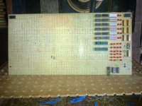
Here is the Reworked Board..

002.jpg

THANK YOU Marty
 
Last edited:
That's funny - I get "There are no items to display."

smp

To clarify:

I used the link in Marty's post and was told I needed to register, just like he said we would. So I registered, retried the link and hit the dead end you hit. But I was able to rummage around and after some flailing about I found the documents. Later I tried the other link that pbirkel supplied and it took me directly to the documents.
 
Marty & DDS, thanks for the clarification. I'll go and rummage around.

smp

UPDATE:
I finally got there... Yes, the URL is exactly as was stated. I have no idea why I had so much trouble, but I'm there now.
 
Last edited:
Thanks Marty.

The link seems to work OK for me.

I will download the files and have a look when I get a few minutes.

Dave
 
Marty,

I downloaded the documents this afternoon and had a quick scan through them.

A couple of things came to mind:

1. What did you do with the two wire lists?

If it was me - I would have manually typed them into a spreadsheet and done some cross-checking between the two of them to ensure that what was typed was sensible. For example, if you couldn't read something from one printout - you may have been able to have read it from the other. I assume that both wiring lists were generated from the same source - but that is not guaranteed. I see someone has hand-edited one of them. I have checked one instance of a hand-edit (P1-60) and the two wiring lists seem to refer to the same 'chain of wires' so this hand-edit does not introduce a functional change. If you had the wiring list(s) as a spreadsheet - you could sort it according to 'signal' so that all the same signals should occur together. I suspect that some of the signal names may be mistyped in some places though.

2. Checkout the registers / big mix and ALU separately.

FIG LD1 on PDF page 7 of "LD8-LD23 Schematics".pdf shows the register layout, the large MUX gate and the ALU. This is the 'heart' of the machine. I would remove all of the peripheral chips - just leaving these in place. You should then be able to bring out the 'inputs' to the remaining chips and test out the various paths with a simple 1 Hz clock and some switches. Have you done this already?

For example, you can set up the MUX gate to enable the SR switches (MUX CONTROL=5) and set the ALU for PASS (M, S0..S1 and CIN) and what you get out of the ALU should be whatever you enter on the switch register. By applying the relevant CLK and /CLR signals to the appropriate register - you should be able to latch the F outputs from the ALU into the selected register. Note that there are some extra inputs for AC to do with rotating - so you will need to set these to LATCH the input into the AC register for now. You should be able to exercise AC SHIFT LEFT and AC SHIFT RIGHT later. You should now be in a position to latch different values into the different registers (SR->MUX->ALU(PASS)->desired register); and then ensure that each register correctly passes through the 1 of 8 MUX gate. Then you can exercise the ALU by taking the SR->MUX->ALU(A) and AC->ALU(B) and using various combinations of the M, S0..S3 and CIN signals to ensure the correct thing happens in going through the ALU.

As the memory is connected between MA/MB and MUX(6) you should also be able to exercise the memory as well.

Only when this works in 'single-step' mode should you move on.

Document the results from each step. In fact, identify what the expected response is first (before you try the test) and ensure you get what you expect. If you don't - go back to the IC data sheets and check that you have understood what should happen. When I tried this step on my simulation of the LD30 I realised I had misunderstood how the ALU works with CIN. I had the operation inverted in my mind!

You should then be able to try something like "take AC, use the ALU to add 1 to it and store the result back in AC". You should then be able to increase the clock speed to the AC register and see what happens. It obviously should count in binary. If it starts to "stutter" as you increase the clock - you may have some noise-indices problems somewhere (or floating inputs to ICs). You may need to wire up some drivers and LEDs to see the pattern on the output from the MUX and ALU. You may have to video the LEDs if you don't have a scope or a logic analyser and play it back at slow speed to ensure that the counting is working properly. If the ALU will add 1 to the 'A' input (i.e. the output from the multiplexer) you should be able to try this test with all of the registers. I haven't got the ALU data sheet handy at the moment.

I don't know how much of this you have already done - so I may be covering 'old ground' for you?

Dave
 
Back
Top