• Please review our updated Terms and Rules here

Commodore P500

If I have an 8-bit that basically boots but hangs, I would be going down the faulty RAM route now. On the insectria site there was a nice suggestion about removing the BASIC ROM. This means the computer boots into the monitor. You can then start selectively filling memory with various bit patterns to try and determine the issue. It's possible that if it is memory, and it affects the zero or stack pages, that the monitor will probably hang as well. At that point I would resort to making a bespoke kernal that does some very basic RAM checks, thought I don't know whether is is possible for you.

Regarding replacing your 6525's - do not despair, they are much easier to find than 6509's as they were also used in 1551 disk drives and in Amiga CD-ROM drives. I see them maybe once every few months on ebay, though you might want to include worldwide in your search criteria.

+1 for what KC9UDX said. Just practise on junk boards. If you are not certain that the chip is dead or not easily replaceable, never cut the pins as most will survive a de-soldering. The odd broken trace or via (the holes in the pcb, which are usually plated through) can be easily spotted and fixed once the chip is removed. My technique is to use a Weller 35W iron with a chisel tip, which is not temperature controlled, and a pump action solder sucker. I heat each pin until the solder visually melts, plus about 1 second, then suck. After doing all 40 pins, flip the board and using quick applications of the iron, push the legs inwards along both sides of the chip and you usually feel a soft click as the leg frees itself from the outside wall of the via. Most new chips have the legs spread outwards so even after sucking, the legs will often still be attached to the outside with the small amount of residual solder. I then work along each pin checking it is free, using a small screwdriver. You can then usually insert a screwdriver under one end of the chip and it will come free with a gentle twist at both ends. A *small* amount of force is OK here but it should not need much. If it isn't coming free, recheck each pin and repeat as required.

You will very occasionally find an obstinate bugger that needs a bit more persuasion, this is when you can find that traces get lifted or a via gets pulled out on the leg of the chip. You should perform a careful visual check of the legs of the pin to see if any via's have been pulled out and the board to check for lifted, broken traces. I usually clean up the board with braid and then PCB cleaner after removing the chip and this makes it much easier to spot faults. If you have, just make a note of where the traces run and fix with fine cored wire on the back side of the board once the socket is fitted.

Hope this helps, Rob

Thanks for the pointers Rob I will take a look at the RAM next, thanks also for the extra info on removing the chips I'm definitely going to get practicing now and exorcise those demons!
 
If I have an 8-bit that basically boots but hangs, I would be going down the faulty RAM route now. On the insectria site there was a nice suggestion about removing the BASIC ROM. This means the computer boots into the monitor. You can then start selectively filling memory with various bit patterns to try and determine the issue. It's possible that if it is memory, and it affects the zero or stack pages, that the monitor will probably hang as well. At that point I would resort to making a bespoke kernal that does some very basic RAM checks, thought I don't know whether is is possible for you.

Rob I've removed the basic ROM's and the computer boots into "monitor 1.0"

I type M 0000 etc and that location appears on the next line.

That's where I get stuck on how to use the monitor to fill the memory for testing/debug purposes as I've never used one before
 
OK, my bad - I thought the monitor had a Fill command, but it doesn't. Here's a link to the B series reference guide from Steve's site which includes a summary of the monitor commands on pages 114-116.

You can still use the M command to show memory and then use the cursor keys to overtype the values, press return to store them and then M again to read the values back. The other important command is V nn, which changes the RAM bank the monitor is looking at. You'll need to check 'v 00' (the vic-II bank), 'v 01' (the main memory) and 'v 0f' (the system bank.) Banks 0 & 1 are 64k, so all the way from 0000-ffff and bank f is only 2k, so 0000-07ff

Put in bit patterns such as $00, $55, $aa and $ff and check identical values are still there when you read them back. You could also just do an 'm 0000 ffff' in banks 00 and 01 and look for obvious deviations from the results of the power on RAM test. You should see alternating 64-byte sequences of 00 and ff.

In bank 0f you'll see a bit more as there's many system locations. For reference, here's the first 1k as appears in VICE after a cold boot. You should see something very similar.

Rob

>C:0000 0f 0f 00 00 00 00 00 00 00 00 00 00 00 00 00 00 ................
>C:0010 00 00 00 00 00 00 00 00 00 00 00 00 00 00 00 00 ................
>C:0020 00 00 00 00 00 00 00 00 00 00 00 00 00 00 00 00 ................
>C:0030 00 00 00 00 00 00 00 00 00 00 00 00 00 00 00 00 ................
>C:0040 00 00 00 00 00 00 00 00 00 00 00 00 00 00 00 00 ................
>C:0050 00 00 00 00 00 00 00 00 00 00 00 00 00 00 00 00 ................
>C:0060 00 00 00 00 00 00 00 00 00 00 00 00 00 00 00 00 ................
>C:0070 00 00 00 00 00 00 00 00 00 00 00 00 00 00 00 00 ................
>C:0080 00 00 00 00 00 00 00 00 00 00 00 00 00 00 00 00 ................
>C:0090 00 02 0f 09 fb 00 00 00 00 00 00 00 00 00 00 00 ................
>C:00a0 00 00 03 00 00 ff 00 00 ff 3f 00 00 00 00 00 00 .........?......
>C:00b0 00 00 00 00 fe 02 00 fb f8 00 02 ff 01 00 00 08 ................
>C:00c0 00 fd 00 00 c0 d3 c0 d7 c0 d3 18 00 02 ff 00 18 ................
>C:00d0 00 00 00 00 20 1d 00 03 0f 02 00 0d 00 18 00 27 .... ..........'
>C:00e0 ff ff 00 00 00 00 00 04 c0 d7 06 00 06 06 06 0f ................
>C:00f0 00 00 00 00 00 00 00 00 00 00 00 00 00 00 00 00 ................
>C:0100 f0 00 00 00 00 00 00 00 00 00 00 00 00 00 00 00 ................
>C:0110 00 00 00 00 00 00 00 00 00 00 00 00 00 00 00 00 ................
>C:0120 00 00 00 00 00 00 00 00 00 00 00 00 00 00 00 00 ................
>C:0130 00 00 00 00 00 00 00 00 00 00 00 00 00 00 00 00 ................
>C:0140 ff ff ff ff ff ff ff ff ff ff ff ff ff ff ff ff ................
>C:0150 ff ff ff ff ff ff ff ff ff ff ff ff ff ff ff ff ................
>C:0160 ff ff ff ff ff ff ff ff ff ff ff ff ff ff ff ff ................
>C:0170 ff ff ff ff ff ff ff ff ff ff ff ff ff ff ff ff ................
>C:0180 00 00 00 00 00 00 00 00 00 00 00 00 00 00 00 00 ................
>C:0190 00 00 00 00 00 00 00 00 00 00 00 00 00 00 00 00 ................
>C:01a0 00 00 00 00 00 00 00 00 00 00 00 00 00 00 00 00 ................
>C:01b0 00 00 00 00 00 00 00 00 00 00 00 00 00 00 00 00 ................
>C:01c0 ff ff ff ff ff ff ff ff ff ff ff ff ff ff ff ff ................
>C:01d0 ff ff ff ff ff ff 42 e9 94 fc 42 e9 94 fc 0f 02 ......B...B.....
>C:01e0 42 42 e9 94 fc 0f 0f 1f e2 20 0f 1f e2 20 42 e9 BB....... ... B.
>C:01f0 94 fc 0f 00 46 00 62 2a e1 46 00 be f4 6b ee ff ....F.b*.F...k..
>C:0200 00 00 00 00 00 00 00 00 00 00 00 00 00 00 00 00 ................
>C:0210 00 00 00 00 00 00 00 00 00 00 00 00 00 00 00 00 ................
>C:0220 00 00 00 00 00 00 00 00 00 00 00 00 00 00 00 00 ................
>C:0230 00 00 00 00 00 00 00 00 00 00 00 00 00 00 00 00 ................
>C:0240 00 00 00 00 00 00 00 00 00 00 00 00 00 00 00 00 ................
>C:0250 00 00 00 00 00 00 00 00 00 00 00 00 00 00 00 00 ................
>C:0260 00 00 00 00 00 00 00 00 00 00 00 00 00 00 00 00 ................
>C:0270 00 00 00 00 00 00 00 00 00 00 00 00 00 00 00 00 ................
>C:0280 00 00 00 00 00 00 00 00 00 00 00 00 00 00 00 00 ................
>C:0290 00 00 00 00 00 00 00 00 00 00 00 00 00 00 00 00 ................
>C:02a0 00 00 00 00 00 00 00 00 00 00 00 00 00 00 00 00 ................
>C:02b0 00 00 00 00 00 00 00 00 00 00 00 00 00 00 00 00 ................
>C:02c0 00 00 00 00 00 00 00 00 00 00 00 00 00 00 00 00 ................
>C:02d0 00 00 00 00 00 00 00 00 00 00 00 00 00 00 00 00 ................
>C:02e0 00 00 00 00 00 00 00 00 00 00 00 00 00 00 00 00 ................
>C:02f0 00 00 00 00 00 00 00 00 00 00 00 00 00 00 00 00 ................
>C:0300 f8 fb 21 ee b8 fc c6 f6 f4 f5 50 f5 aa f5 ad f6 ..!.......P.....
>C:0310 a3 f4 f5 f4 72 f9 44 f4 86 f6 4d f7 53 f8 73 ee ....r.D...M.S.s.
>C:0320 1f e0 1f e0 7b f2 87 f2 11 f3 9e f2 b2 f2 b6 f2 ....{...........
>C:0330 3b f2 37 f2 00 00 00 00 00 00 00 00 00 00 00 00 ;.7.............
>C:0340 00 00 00 00 00 00 00 00 00 00 00 00 00 00 00 00 ................
>C:0350 00 00 02 00 00 ff fc 01 02 00 00 ff fb 01 00 00 ................
>C:0360 00 c0 00 00 00 00 4d 00 00 00 6b fe 00 00 00 00 ......M...k.....
>C:0370 00 00 00 00 00 00 00 00 00 00 00 00 00 00 00 00 ................
>C:0380 ff fe 01 00 18 0d 00 00 00 00 00 00 0f 05 04 06 ................
>C:0390 06 05 06 04 09 07 05 00 00 00 00 00 00 00 00 00 ................
>C:03a0 00 00 00 00 00 00 00 00 00 00 00 00 00 00 00 00 ................
>C:03b0 00 00 00 00 00 f6 e9 41 e6 50 e6 39 e0 39 e0 00 .......A.P.9.9..
>C:03c0 00 00 00 00 00 00 00 00 00 00 00 00 00 00 00 00 ................
>C:03d0 00 00 00 00 00 00 00 00 00 00 00 00 00 00 00 00 ................
>C:03e0 00 00 00 00 00 00 00 00 00 00 00 00 00 00 00 00 ................
>C:03f0 00 00 00 00 00 00 00 00 00 ee a5 5a ff ff ff ff ...........Z....
 
Last edited:
OK, my bad - I thought the monitor had a Fill command, but it doesn't. Here's a link to the B series reference guide from Steve's site which includes a summary of the monitor commands on pages 114-116.

You can still use the M command to show memory and then use the cursor keys to overtype the values, press return to store them and then M again to read the values back. The other important command is V nn, which changes the RAM bank the monitor is looking at. You'll need to check 'v 00' (the vic-II bank), 'v 01' (the main memory) and 'v 0f' (the system bank.) Banks 0 & 1 are 64k, so all the way from 0000-ffff and bank f is only 2k, so 0000-07ff

Put in bit patterns such as $00, $55, $aa and $ff and check identical values are still there when you read them back. You could also just do an 'm 0000 ffff' in banks 00 and 01 and look for obvious deviations from the results of the power on RAM test. You should see alternating 64-byte sequences of 00 and ff.

In bank 0f you'll see a bit more as there's many system locations. For reference, here's the first 1k as appears in VICE after a cold boot. You should see something very similar.

Rob

>C:0000 0f 0f 00 00 00 00 00 00 00 00 00 00 00 00 00 00 ................
>C:0010 00 00 00 00 00 00 00 00 00 00 00 00 00 00 00 00 ................
>C:0020 00 00 00 00 00 00 00 00 00 00 00 00 00 00 00 00 ................
>C:0030 00 00 00 00 00 00 00 00 00 00 00 00 00 00 00 00 ................
>C:0040 00 00 00 00 00 00 00 00 00 00 00 00 00 00 00 00 ................
>C:0050 00 00 00 00 00 00 00 00 00 00 00 00 00 00 00 00 ................
>C:0060 00 00 00 00 00 00 00 00 00 00 00 00 00 00 00 00 ................
>C:0070 00 00 00 00 00 00 00 00 00 00 00 00 00 00 00 00 ................
>C:0080 00 00 00 00 00 00 00 00 00 00 00 00 00 00 00 00 ................
>C:0090 00 02 0f 09 fb 00 00 00 00 00 00 00 00 00 00 00 ................
>C:00a0 00 00 03 00 00 ff 00 00 ff 3f 00 00 00 00 00 00 .........?......
>C:00b0 00 00 00 00 fe 02 00 fb f8 00 02 ff 01 00 00 08 ................
>C:00c0 00 fd 00 00 c0 d3 c0 d7 c0 d3 18 00 02 ff 00 18 ................
>C:00d0 00 00 00 00 20 1d 00 03 0f 02 00 0d 00 18 00 27 .... ..........'
>C:00e0 ff ff 00 00 00 00 00 04 c0 d7 06 00 06 06 06 0f ................
>C:00f0 00 00 00 00 00 00 00 00 00 00 00 00 00 00 00 00 ................
>C:0100 f0 00 00 00 00 00 00 00 00 00 00 00 00 00 00 00 ................
>C:0110 00 00 00 00 00 00 00 00 00 00 00 00 00 00 00 00 ................
>C:0120 00 00 00 00 00 00 00 00 00 00 00 00 00 00 00 00 ................
>C:0130 00 00 00 00 00 00 00 00 00 00 00 00 00 00 00 00 ................
>C:0140 ff ff ff ff ff ff ff ff ff ff ff ff ff ff ff ff ................
>C:0150 ff ff ff ff ff ff ff ff ff ff ff ff ff ff ff ff ................
>C:0160 ff ff ff ff ff ff ff ff ff ff ff ff ff ff ff ff ................
>C:0170 ff ff ff ff ff ff ff ff ff ff ff ff ff ff ff ff ................
>C:0180 00 00 00 00 00 00 00 00 00 00 00 00 00 00 00 00 ................
>C:0190 00 00 00 00 00 00 00 00 00 00 00 00 00 00 00 00 ................
>C:01a0 00 00 00 00 00 00 00 00 00 00 00 00 00 00 00 00 ................
>C:01b0 00 00 00 00 00 00 00 00 00 00 00 00 00 00 00 00 ................
>C:01c0 ff ff ff ff ff ff ff ff ff ff ff ff ff ff ff ff ................
>C:01d0 ff ff ff ff ff ff 42 e9 94 fc 42 e9 94 fc 0f 02 ......B...B.....
>C:01e0 42 42 e9 94 fc 0f 0f 1f e2 20 0f 1f e2 20 42 e9 BB....... ... B.
>C:01f0 94 fc 0f 00 46 00 62 2a e1 46 00 be f4 6b ee ff ....F.b*.F...k..
>C:0200 00 00 00 00 00 00 00 00 00 00 00 00 00 00 00 00 ................
>C:0210 00 00 00 00 00 00 00 00 00 00 00 00 00 00 00 00 ................
>C:0220 00 00 00 00 00 00 00 00 00 00 00 00 00 00 00 00 ................
>C:0230 00 00 00 00 00 00 00 00 00 00 00 00 00 00 00 00 ................
>C:0240 00 00 00 00 00 00 00 00 00 00 00 00 00 00 00 00 ................
>C:0250 00 00 00 00 00 00 00 00 00 00 00 00 00 00 00 00 ................
>C:0260 00 00 00 00 00 00 00 00 00 00 00 00 00 00 00 00 ................
>C:0270 00 00 00 00 00 00 00 00 00 00 00 00 00 00 00 00 ................
>C:0280 00 00 00 00 00 00 00 00 00 00 00 00 00 00 00 00 ................
>C:0290 00 00 00 00 00 00 00 00 00 00 00 00 00 00 00 00 ................
>C:02a0 00 00 00 00 00 00 00 00 00 00 00 00 00 00 00 00 ................
>C:02b0 00 00 00 00 00 00 00 00 00 00 00 00 00 00 00 00 ................
>C:02c0 00 00 00 00 00 00 00 00 00 00 00 00 00 00 00 00 ................
>C:02d0 00 00 00 00 00 00 00 00 00 00 00 00 00 00 00 00 ................
>C:02e0 00 00 00 00 00 00 00 00 00 00 00 00 00 00 00 00 ................
>C:02f0 00 00 00 00 00 00 00 00 00 00 00 00 00 00 00 00 ................
>C:0300 f8 fb 21 ee b8 fc c6 f6 f4 f5 50 f5 aa f5 ad f6 ..!.......P.....
>C:0310 a3 f4 f5 f4 72 f9 44 f4 86 f6 4d f7 53 f8 73 ee ....r.D...M.S.s.
>C:0320 1f e0 1f e0 7b f2 87 f2 11 f3 9e f2 b2 f2 b6 f2 ....{...........
>C:0330 3b f2 37 f2 00 00 00 00 00 00 00 00 00 00 00 00 ;.7.............
>C:0340 00 00 00 00 00 00 00 00 00 00 00 00 00 00 00 00 ................
>C:0350 00 00 02 00 00 ff fc 01 02 00 00 ff fb 01 00 00 ................
>C:0360 00 c0 00 00 00 00 4d 00 00 00 6b fe 00 00 00 00 ......M...k.....
>C:0370 00 00 00 00 00 00 00 00 00 00 00 00 00 00 00 00 ................
>C:0380 ff fe 01 00 18 0d 00 00 00 00 00 00 0f 05 04 06 ................
>C:0390 06 05 06 04 09 07 05 00 00 00 00 00 00 00 00 00 ................
>C:03a0 00 00 00 00 00 00 00 00 00 00 00 00 00 00 00 00 ................
>C:03b0 00 00 00 00 00 f6 e9 41 e6 50 e6 39 e0 39 e0 00 .......A.P.9.9..
>C:03c0 00 00 00 00 00 00 00 00 00 00 00 00 00 00 00 00 ................
>C:03d0 00 00 00 00 00 00 00 00 00 00 00 00 00 00 00 00 ................
>C:03e0 00 00 00 00 00 00 00 00 00 00 00 00 00 00 00 00 ................
>C:03f0 00 00 00 00 00 00 00 00 00 ee a5 5a ff ff ff ff ...........Z....

Hi again Rob thanks for the info, I used the monitor to check v00 v01 v0f memory and the first two bits won't save there correct value

>C:0000 0f 01 00 00 00 00 00 00

if I use the monitor to alter the values to:

>C:0000 ff ff ff ff ff ff ff ff

I get

>c:0000 0f 0f ff ff ff ff ff ff

also

>c:0090 00 02 0f ff ff ff ff ff
>c:0098 ff ff ff ff ff ff 00 ff ff
>c:00a0 ff 00 03 ff ff ff ff 00

How do I know which ram chip that equates to?
 
Last edited:
A few videos of the monitor listings:-

[video]http://vid984.photobucket.com/albums/ae322/SX-64_USER/P500/2015-02-20_17-50-02_624.mp4[/video]

[video]http://vid984.photobucket.com/albums/ae322/SX-64_USER/P500/2015-02-20_17-46-44_644.mp4[/video]

[video]http://vid984.photobucket.com/albums/ae322/SX-64_USER/P500/2015-02-20_17-45-40_670.mp4[/video]

Oh! and a video of the actual faults

[video]http://vid984.photobucket.com/albums/ae322/SX-64_USER/2015-02-20_17-52-53_827.mp4[/video]
 
Last edited:
Just had a look at WinVice as I didn't realise the P500 was on there until crock mentioned it.

I was wondering if the delay time on start up was normal as my P500 boots in about one second where as in WinVice it takes about eight seconds on hard reset?
 
Just had a look at WinVice as I didn't realise the P500 was on there until crock mentioned it.

I was wondering if the delay time on start up was normal as my P500 boots in about one second where as in WinVice it takes about eight seconds on hard reset?
That points very strongly to RAM problems or possibly one of PLA's, as they control RAS and CAS. The delay is the kernal doing a RAM test. It stops when it finds a problem I think. I will reply later in more detail but I'm at the kids sports event ATM.
 
Hi again Rob thanks for the info, I used the monitor to check v00 v01 v0f memory and the first two bits won't save there correct value

>C:0000 0f 01 00 00 00 00 00 00

if I use the monitor to alter the values to:

>C:0000 ff ff ff ff ff ff ff ff

I get

>c:0000 0f 0f ff ff ff ff ff ff

Locations $00 and $01 are not RAM they are IO ports on the 6509 cpu. The normal value for these is $0F which means BANK 15, which is the system BANK. SYSTEM RAM, BASIC, KERNAL, SCREEN and IO are in BANK 15.
Location $00 is the "execution register" which controls which bank is actually running code. Location $01 is the "indirection register" which is the bank used for DATA retrieval using a pair of modified opcodes.

Steve
 
That points very strongly to RAM problems or possibly one of PLA's, as they control RAS and CAS. The delay is the kernal doing a RAM test. It stops when it finds a problem I think. I will reply later in more detail but I'm at the kids sports event ATM.

Both PLA's read ok on the programmer so does that rule them out?
Thanks Rob more detail will be appreciated

Locations $00 and $01 are not RAM they are IO ports on the 6509 cpu. The normal value for these is $0F which means BANK 15, which is the system BANK. SYSTEM RAM, BASIC, KERNAL, SCREEN and IO are in BANK 15.
Location $00 is the "execution register" which controls which bank is actually running code. Location $01 is the "indirection register" which is the bank used for DATA retrieval using a pair of modified opcodes.

Steve

Hi Steve I'm having a bit of a problem understanding the memory areas.

Regarding RAM am I right in saying that the 2k static Ram U85 by the Kernal ROM, BASIC ROM's is v0f

The RAM chips U66-u73 are v00
The RAM chips U33-U40 are v01

or is this wide of the mark?

On the monitor do the 8 bits relate to each 8 4164 RAM chips as the bits are shared between the 8 chips making the byte?
>c:0000 00 00 00 00 00 first byte
>c:0008 00 00 00 00 00 second byte

bit 0 stored in U73
bit 1 stored in U72
bit 2 stored in U71
bit 3 stored in U70
bit 4 stored in U69
bit 5 stored in U68
bit 6 stored in U67
bit 7 stored in U66

I'm proper confused regarding $00 and $01 so they are not in the RAM locations

Oh and are the BANK's inside the 64k RAM (u66-U73) or are each 64k RAM area (U66-73 & U33-U40) a BANK?

Sorry for all the questions
 
The P500 and CBM-II machines have a 6509 processor, which extends memory by organizing it into banks of 64K RAM. It can have 16 banks for a total of 1 megabyte. When the CPU resets it defaults to bank 15. Locations $0 and $1 are inside the processor and appear in EVERY bank. Location $0 is the execution register which controls which bank is running code. If you modify this register the CPU will immediately start using the new bank... it does not even change the address of the Program Counter (PC) which is 16-bit only. Location $01 is the indirection register and it allows the CPU to access memory in any bank WITHOUT changing the bank where code is executing. So for example, all ROM is in BANK 15, and the KERNAL and BASIC ROMs are there. The processor executes code in BANK 15 but when it needs to access the BASIC program or variables it changes $01 to "fetch" or "store" bytes in BANK 1.

There is 2K of RAM starting at $0000 in BANK15. This is used for the system zero page, stack and operating system storage. This is the 2K x8 static ram (2016) chip at U85. Also in BANK 15 is 1.5K of 2114 (1Kx4) dynamic RAM chips for video memory at U24 (color ram) and U74/U75 (character ram) used by the VIC-II chip.

Memory in BANK 0 to 3 use 64Kx1 dynamic RAM chips:

- BANK 0 = U66 to U73 (accessed by VIC-II for graphics mode)
- BANK 1 = U33 to U40 (where BASIC programs are located)
- BANK 2 = U41 to U48 (normally not installed)
- BANK 3 = U58 to U65 (also not installed).

So, yes, it takes all 8 dynamic ram chips to store a complete byte.

Steve
 
I think I am understanding it better now Steve so:-
BANK 0 is v00 and that is only used by the VIC-II for any graphics
BANK 1 is V01 where the BASIC programs are stored and BANKS 2 & 3 would be if the board was fully populated like the B256 and any expansions
would be in BANK 4-14.
BANK 15 is v0f is the static where KERNAL and BASIC roms reside and the zero page etc... and video RAMS.

Do the RAM BANKs get checked in order BANK 0 then 1 etc to 15?

Regarding my videos in post #25:-

Would I be right in saying that my problems lie in BANK 0 v00 (U66-U73) because the RAM has a lot garbage or could this be due to the checks failing higher
in the BANK 1 RAM locations as the RAM check not being completed?
BASIC is booting to startup up banner but could there still be a problem with the system memory BANK 15 v0f as no commands work and BANK 15 is also full
of garbage further up the monitor.
BANK 1 v01 looks like the RAMs have been checked as they are all mainly 00 & ff with the odd garbage result but I haven't checked further up the monitor.

Checking in WinVice BANKs 0,1 and 15 have clean looking RAMs with rows of 00 then ff.

Can I ask you if the ROM daughter board is soldered in place or if it is socketed?
Mine is on green plastic and brass headers but it's either really tight or soldered in one piece?
 
Last edited:
I think I am understanding it better now Steve so:-
BANK 0 is v00 and that is only used by the VIC-II for any graphics
BANK 1 is V01 where the BASIC programs are stored and BANKS 2 & 3 would be if the board was fully populated like the B256 and any expansions
would be in BANK 4-14.
BANK 15 is v0f is the static where KERNAL and BASIC roms reside and the zero page etc... and video RAMS.
That's basically it, yes. Even if banks 2 and 3 were populated though, you would need an alternative basic and kernal ROM to make use of it. The other B-series machines have separate ROM's for the 128k and 256k machines. As far as I am aware, there is only the one official version of the P500 ROM's.

Do the RAM BANKs get checked in order BANK 0 then 1 etc to 15?
I just looked through the code and yes, it starts at bank 0 and goes up to 14, looking for the first one to fail. The highest successful bank tested is stored in $0357. If you look in my printout or in VICE, that contains $01. In your video, it contains $FF, meaning the ram test of bank $00 failed. It doesn't check the system bank in this routine.

BASIC is booting to startup up banner but could there still be a problem with the system memory BANK 15 v0f as no commands work and BANK 15 is also full
of garbage further up the monitor.
Bank 15 only goes as far as $0800, and it looks OK to me. As Steve said, this is where your ZP and Stack are and if these were faulty, you'd most likely be looking at a black screen.
BANK 1 v01 looks like the RAMs have been checked as they are all mainly 00 & ff with the odd garbage result but I haven't checked further up the monitor.

Checking in WinVice BANKs 0,1 and 15 have clean looking RAMs with rows of 00 then ff.
After looking at the startup code, it does not explicitly set $00 and $FF, this is just what VICE initialises it's RAM emulation with. I don't know how consistently that would appear on real hardware.

Can I ask you if the ROM daughter board is soldered in place or if it is socketed?
Mine is on green plastic and brass headers but it's either really tight or soldered in one piece?
I don't have either of my P500's to hand, but from memory, I think it's socketed with a couple of soldered jumper wires.

Rob
 
Thanks for the reply Rob, do you think the daughter board is just a bit stuck from not being moved for a few years?

So if I'm understanding you correctly even if you populated the board to add another 128k to 256k you would need an updated Kernal to use it?

Can you give me a brief description in layman's terms of what the zero page and stack are exactly? (really feel ingnorant asking these basic questions!)

Would faulty RAM in BANK 0 not cause the computer to fail as it's only used for graphic operations or does it not work that way?

I think it may be time to socket the RAM locations and substitute the RAM.

Thanks again for your thorough and detailed replies!
 
Thanks for the reply Rob, do you think the daughter board is just a bit stuck from not being moved for a few years?
Possibly. You should be able to tell from looking underneath the daughter board. If the pins go into what looks like a normal socket, it's probably just stuck. Depending on the design of the pin headers used, they pins are usually much thicker than the legs of a chip, EPROM or otherwise. I'm assuming you have normal EPROM('s) in the daughterboard, so do you really need to remove it anyway?

So if I'm understanding you correctly even if you populated the board to add another 128k to 256k you would need an updated Kernal to use it?
For BASIC to make use of it yes. In the other 256k machines, code is stored in bank 0, while variables, arrays and strings go into banks 1,2 & 3 (don't recall exactly which in which) while in a 128k machine, code is in 0 and *all* variables are in bank 1.

There's 2 offical versions of the ROM sets with the suffix -01 and -02 but the only difference is bug fixes to my knowledge. It's possible someone has done a homebrew version for 256k though. On the otherhand, you could write your own programs to make use of it without any changes to the ROM's.

Can you give me a brief description in layman's terms of what the zero page and stack are exactly? (really feel ingnorant asking these basic questions!)
Of course, we all had to start somewhere. :)

The ZeroPage refers to the first 256 bytes of memory, so from locations $0000 -> $00ff. These are special for all the 6502 based processors because there is a number of instructions which are desiged to make use of it for more efficient performance. For example LDA $00ff (absolute addressing) takes 3 bytes of storage and takes 4 cycles to execute, whereas LDA $ff (zeropage addressing) takes 2 bytes and 3 cycles to execute.

On top of this, there is also the indexed indirect addressing modes which allow you to manipulate memory via pointers in the zero page. One of the supposed shortcomings of the 6502 highlighted by its detractors was the lack of registers, but in fact you have 256 of them in the zero page.

The stack resides at positions $0100 -> $01ff and is the processors temporary storage area for return addresses when executing subroutines. As a side effect, it then allows for an elegant way to handle parameters and returned values from subroutines. It can also be used as a generic storage area by pushing and pulling values on and off the stack with the PHA and PLA instructions. The processor maintains a 'stack pointer' which points to the next available position on the stack. The very first instructions executed on a 6502 based machine on power up is usually LDX #$FF, TXS to initialise it.

As the stack, and to a lesser extent the ZP, are so crucial to the operation of the 6502 based machines, it's unlikely you'll see much if those areas of memory are failed, as you can't even use a JSR instruction.

Would faulty RAM in BANK 0 not cause the computer to fail as it's only used for graphic operations or does it not work that way?
I really don't know. You might be able to configure the P500 emulation in VICE to test the effect. I will try later tonight.

I think it may be time to socket the RAM locations and substitute the RAM.
Lets see if we can nail it down a bit better first. First of all try setting values in bank 0 via the monitor instructions in my previous post. You could also try the old 'finger test' and put your finger on the DRAM's after it's been switched on for a couple of minutes. Failed DRAM's often run very hot. It's also possible that it's one of the multiplexers (74LS257's.)

cheers, Rob
 
Possibly. You should be able to tell from looking underneath the daughter board. If the pins go into what looks like a normal socket, it's probably just stuck. Depending on the design of the pin headers used, they pins are usually much thicker than the legs of a chip, EPROM or otherwise. I'm assuming you have normal EPROM('s) in the daughterboard, so do you really need to remove it anyway?

Well Rob I can confirm it's not socketed they are on fixed headers. What a PITA to remove!


For BASIC to make use of it yes. In the other 256k machines, code is stored in bank 0, while variables, arrays and strings go into banks 1,2 & 3 (don't recall exactly which in which) while in a 128k machine, code is in 0 and *all* variables are in bank 1.

There's 2 offical versions of the ROM sets with the suffix -01 and -02 but the only difference is bug fixes to my knowledge. It's possible someone has done a homebrew version for 256k though. On the otherhand, you could write your own programs to make use of it without any changes to the ROM's.


Of course, we all had to start somewhere. :)

The ZeroPage refers to the first 256 bytes of memory, so from locations $0000 -> $00ff. These are special for all the 6502 based processors because there is a number of instructions which are desiged to make use of it for more efficient performance. For example LDA $00ff (absolute addressing) takes 3 bytes of storage and takes 4 cycles to execute, whereas LDA $ff (zeropage addressing) takes 2 bytes and 3 cycles to execute.

On top of this, there is also the indexed indirect addressing modes which allow you to manipulate memory via pointers in the zero page. One of the supposed shortcomings of the 6502 highlighted by its detractors was the lack of registers, but in fact you have 256 of them in the zero page.

The stack resides at positions $0100 -> $01ff and is the processors temporary storage area for return addresses when executing subroutines. As a side effect, it then allows for an elegant way to handle parameters and returned values from subroutines. It can also be used as a generic storage area by pushing and pulling values on and off the stack with the PHA and PLA instructions. The processor maintains a 'stack pointer' which points to the next available position on the stack. The very first instructions executed on a 6502 based machine on power up is usually LDX #$FF, TXS to initialise it.

As the stack, and to a lesser extent the ZP, are so crucial to the operation of the 6502 based machines, it's unlikely you'll see much if those areas of memory are failed, as you can't even use a JSR instruction.


I really don't know. You might be able to configure the P500 emulation in VICE to test the effect. I will try later tonight.

Thanks for that, very helpful to get me understanding these beasts.


Lets see if we can nail it down a bit better first. First of all try setting values in bank 0 via the monitor instructions in my previous post. You could also try the old 'finger test' and put your finger on the DRAM's after it's been switched on for a couple of minutes. Failed DRAM's often run very hot. It's also possible that it's one of the multiplexers (74LS257's.)

cheers, Rob

The problem in that area is that the RAM chips are covered by the daughter board so even getting a finger on the chips is impossible and so is piggybacking.
another almighty massive problem is that if you socket the RAM in that area the daughterboad will have to be raised, then the EPROM's that already foul the keyboard
is fouled even more so the EPROM's need to be changed to 2364 and do away with the daughter board or have it on a ribbon cable and move to a more accessible
area of the computer.
 
Well Rob I can confirm it's not socketed they are on fixed headers. What a PITA to remove!
Can you post a picture of that? I don't recall mine being that way.
Thanks for that, very helpful to get me understanding these beasts.
You're welcome. As a machine language noob on 8-bit Cmmodore's, this is the best book to read. https://archive.org/details/Machine_Language_for_the_Commodore_Revised_and_Expanded_Edition

The problem in that area is that the RAM chips are covered by the daughter board so even getting a finger on the chips is impossible and so is piggybacking. Another almighty massive problem is that if you socket the RAM in that area the daughterboad will have to be raised, then the EPROM's that already foul the keyboard is fouled even more so the EPROM's need to be changed to 2364 and do away with the daughter board or have it on a ribbon cable and move to a more accessible area of the computer.
Hmm, lets see that picture. I have some super slimline sockets which may help.
 
Some good discussion, sorry I was offline for a while. A couple points. The P500 is the only CBM-II machine with ram in BANK 0. All others start at bank 1. I know in the P500 that the VIC-II can access ram in bank 0 but I don't know what else goes there. I always assumed that basic programs were stored in bank 1 like the rest of the machines, but I'm not 100% sure now. I haven't really worked on my P500 for many years now.

As for 128K vs 256K it is true, for the B-series there are different BASIC ROMS for each configuration. The actual source code is available and commodore also planned a 192K configuration. AFAIK there was only one set of ROMs released for the P500 and it says 128K on startup, so that would indicate that it uses both banks. I'd have to check which bank is used for what. It seem curious that on the motherboard BANK 0 is located separately from BANKs 1 to 3.

Steve
 
Some good discussion, sorry I was offline for a while. A couple points. The P500 is the only CBM-II machine with ram in BANK 0. All others start at bank 1. I know in the P500 that the VIC-II can access ram in bank 0 but I don't know what else goes there. I always assumed that basic programs were stored in bank 1 like the rest of the machines, but I'm not 100% sure now. I haven't really worked on my P500 for many years now.
Just did a bit of experimenting and surprisingly, BASIC code goes into bank 0, variables, strings (and I assume arrays) into bank 1. This would probably explain why the OP's machine hangs if bank 0 is faulty.

As for 128K vs 256K it is true, for the B-series there are different BASIC ROMS for each configuration. The actual source code is available and commodore also planned a 192K configuration.
Would like to see the source code if you have a link. Does it have conditional sections for the different RAM configurations? If so, it might make it easier to construct a true 256k version for the P500.

I'd have to check which bank is used for what. It seem curious that on the motherboard BANK 0 is located separately from BANKs 1 to 3.
Fairly certain the VIC-II can only access bank 0 and I assume that's why it's co-located. Like you, I assumed that it all went into bank 1. It's nice to learn something new.

Rob
 
Thanks for figuring that out. I will have to update my webpage with that info.

The source code for the CBM-II firmware is available on CBUG disks 67-69. Unfortunately the P500-specific screen editor source is missing, but you can see references to the P series in the rest of the code.

http://www.zimmers.net/anonftp/pub/cbm/b/CBUG/index.html

I'm not sure if you'd really want to build other memory configurations though. On the B-series most commercial software required the 128K roms. I also found it was nice to have 2 "unused" ram banks on 128K machines that were upgraded to 256K. Of course for the P500 there IS NO commercial software, so it doesn't really matter, except as an intellectual exercise.

Steve
 
2015-02-24_20-20-59_156.jpg

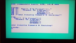
Yes!! I fixed her yesterday but I had to put a few things right I did wrongly (though done with good intentions) :happy2:

The problem was in BANK 0 U71 was faulty. I found the fault by first having to desolder the ROM daughter board, I had to do this because there was not enough clearance
to piggyback the chips on top of the existing ones as the daughter board was too close. If only I had done this first in the first place I wouldn't have had to change the 6525's but they were the main suspect and I could only piggyback 11 out of 16 chips to begin with. Sods law said the faulty ones were under the daughter board.

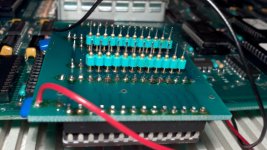
Here is a picture of the headers

2015-02-23_19-48-27_837.jpg

Then very poor decision by me was to socket the RAM chip and the ROM daughter board, I say poorly because it increased the height of the ROM's and they fouled the
keyboard. I was going to use 2364 Eproms but they are as rare as the 6525's 6509 etc... To add insult to injury I removed U70 mistakenly as the daughter board was covering
one RAM chip so when I counted three in it was actually four! After removing the sockets (thanks to the lads advice with a bit of care I did so without a problem!) and then
resoldering the chips and board in place. Why do you always make mistakes when you try your best not too!

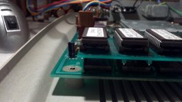
Height picture.

2015-02-23_19-45-02_376.jpg

So it just remains for me to say thanks guys for the assistance very much appreciated!!
 
Last edited:
Back
Top