• Please review our updated Terms and Rules here

Dec H851 pcb redesign

Roland Huisman

Veteran Member
Joined
Mar 24, 2011
Messages
1,464
Location
The Netherlands
So I've had it with the bad PCB's on the H851 top connectors.
Now a second one has a broken trace. I've redesigned the PCB
and ordered a few in China. This offers me also the possibility of
making a few extra H851s from a few single connectors...
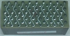
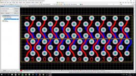
Dec H851.jpg

Dec H851 new.jpg

When I have the PCB's I will let you all know if I succeed.

Regards, Roland
 
So today I finally got my new PCBs for the H851 connectors.
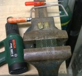
I first divided the PCB into 4 pieces with a little saw. The removed
the pieces of the old PCB by heating it with a paint stripper.

Remove old PCB.jpg

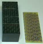
The clean connector and new PCB. (Got 11 spare PCBs now)

ready for new PCB.jpg

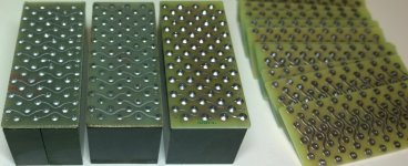
And I've noticed that there are at least two versions of the H851.
The old version (on the left) does not seem to have a plating trough the holes.
Little metal bushes are used here to connect the top and bottom of the PCB.
There are also two separate connectors and those are integrated into one
connector in the newer version. (In the middle)

At the right my new PCB is soldered at the original connector. Brand new again :D

versions.jpg

Now I got my 4 H851 plugs to complete my 4K of memory. YaaaY :D

Regards, Roland
 
A particularly pleasing solder job there with so many perfectly equal blobs over the pins :)
 
Those boards looks really good! I have at least one broken H851 and I planed to do exactly what you did. Did you make any extras that you can sell?
 
Thanks for the complements guys :D

And yes, I've got a few spares! And I can also share the gerber files as well if anyone is interested.

Regards, Roland
 
Last edited:
Back
Top