• Please review our updated Terms and Rules here

DGC Nova 2: looking for parts & info, exchange possible

farjmp

Member
Joined
Dec 29, 2020
Messages
28
Hi All.

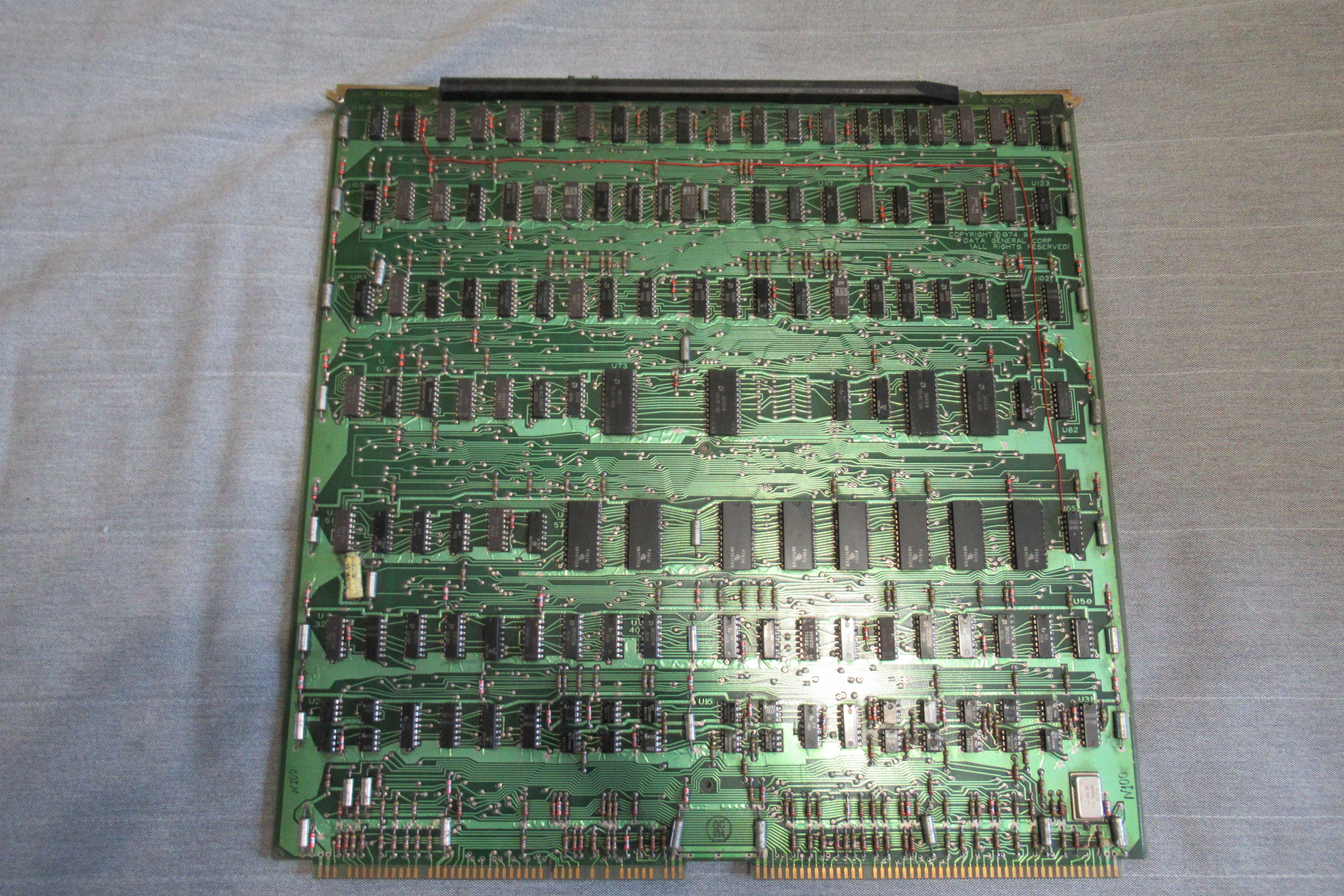
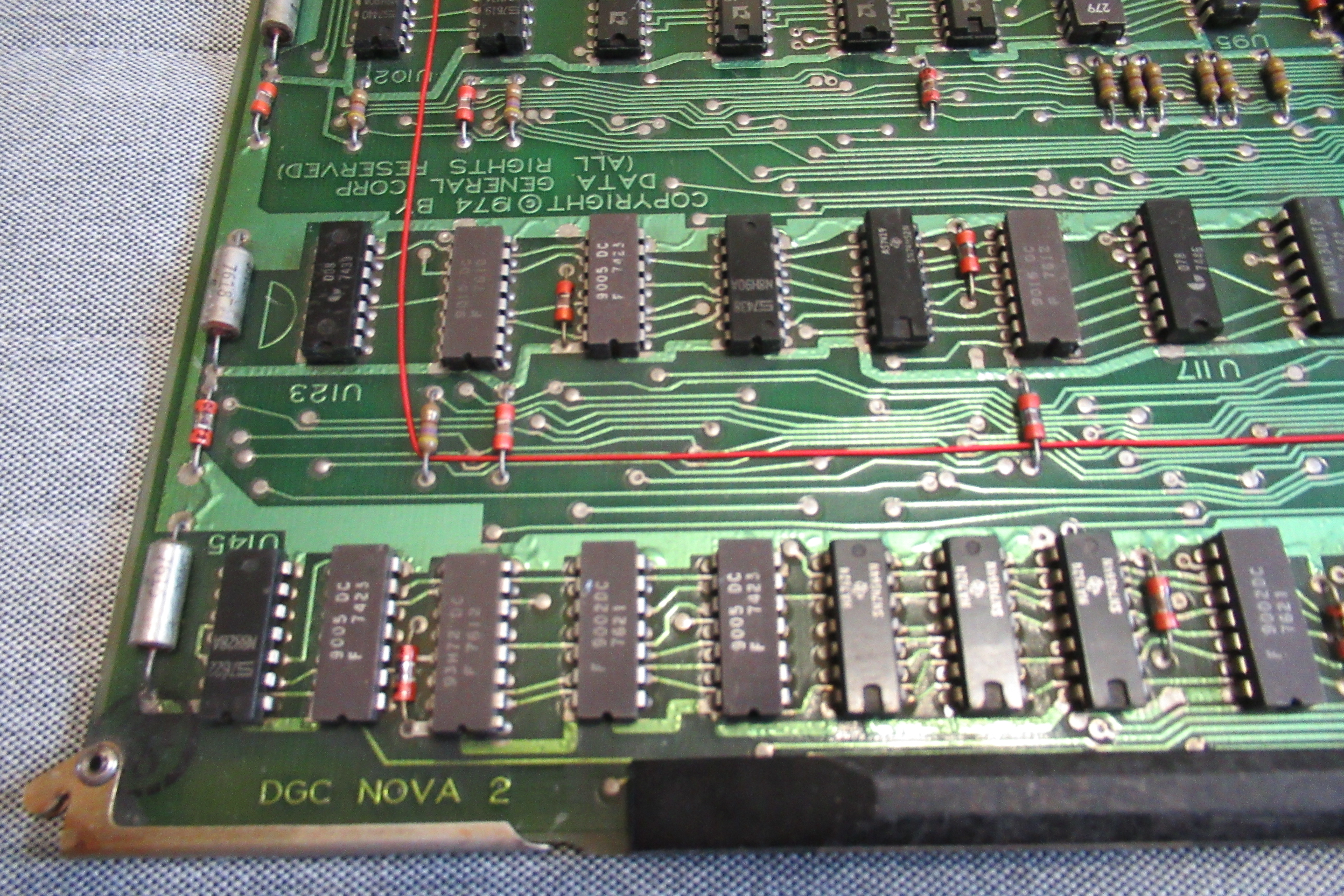
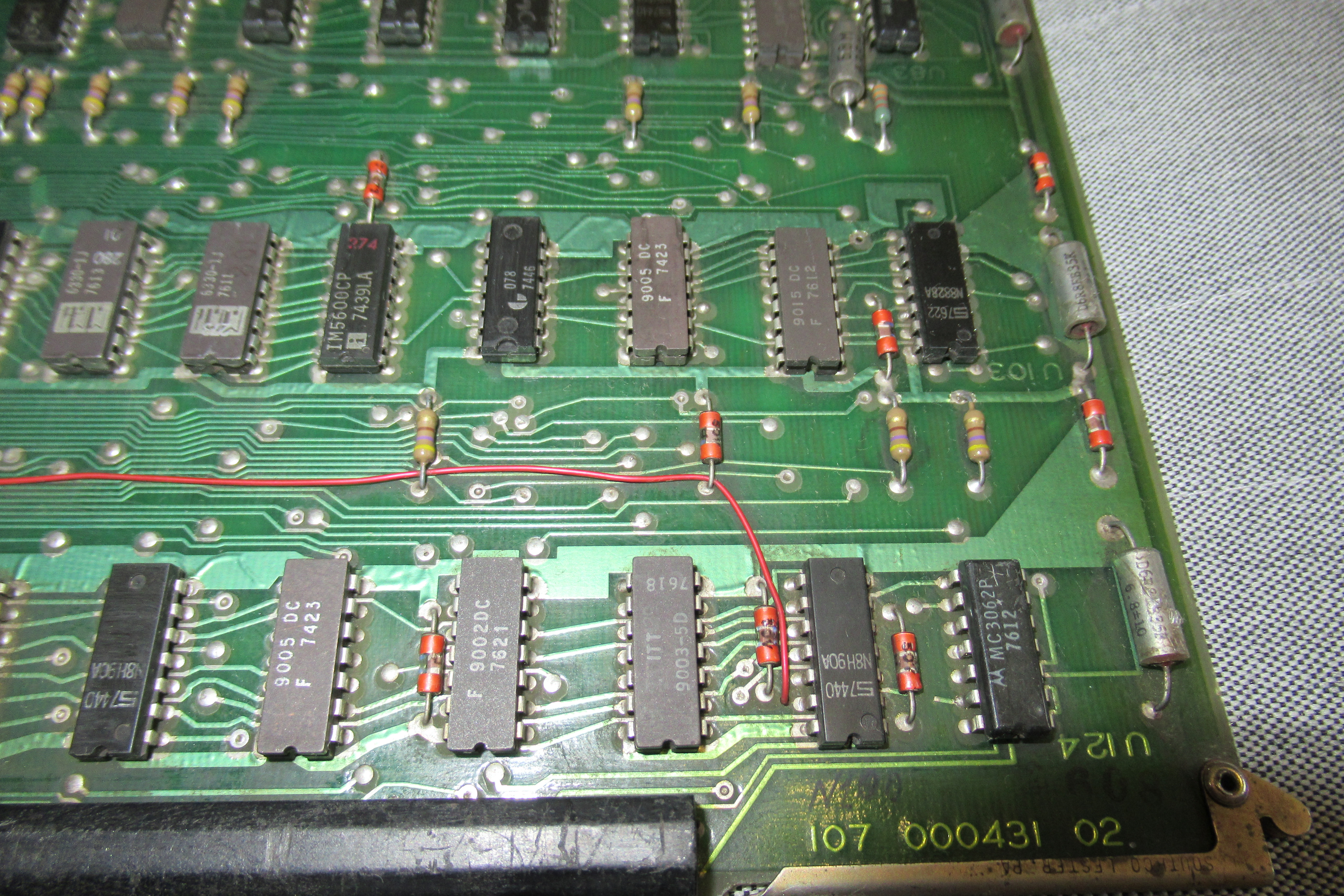
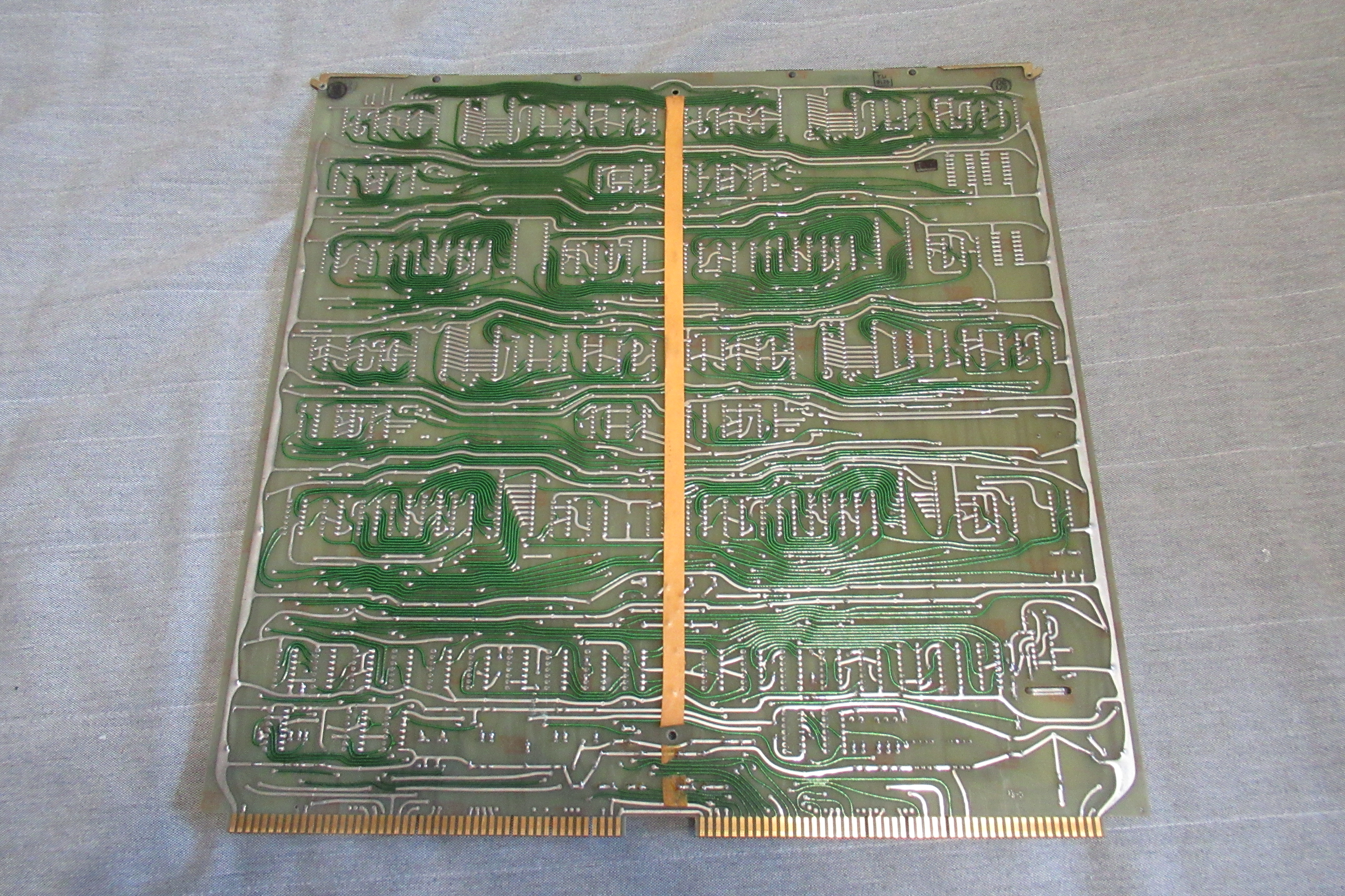
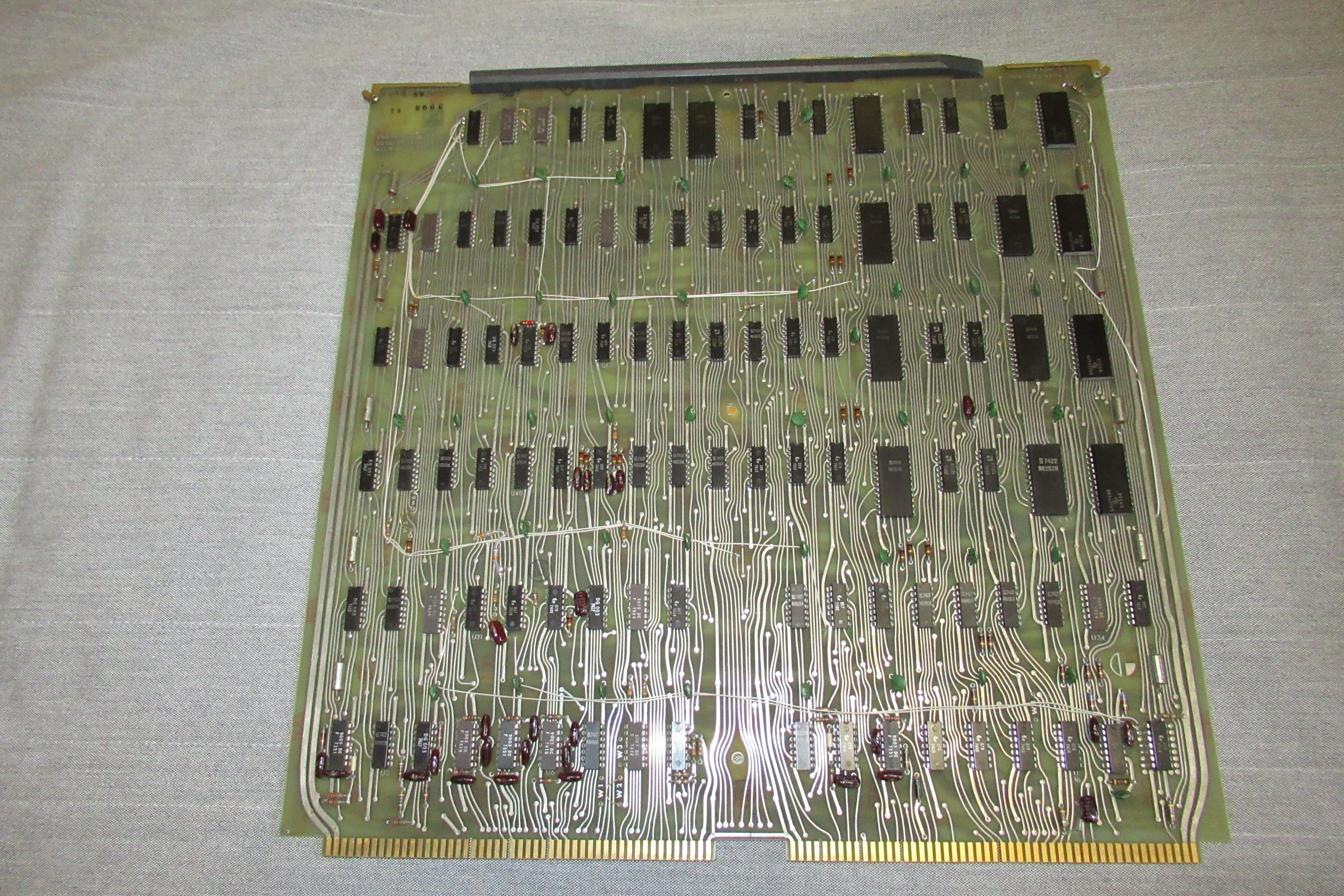
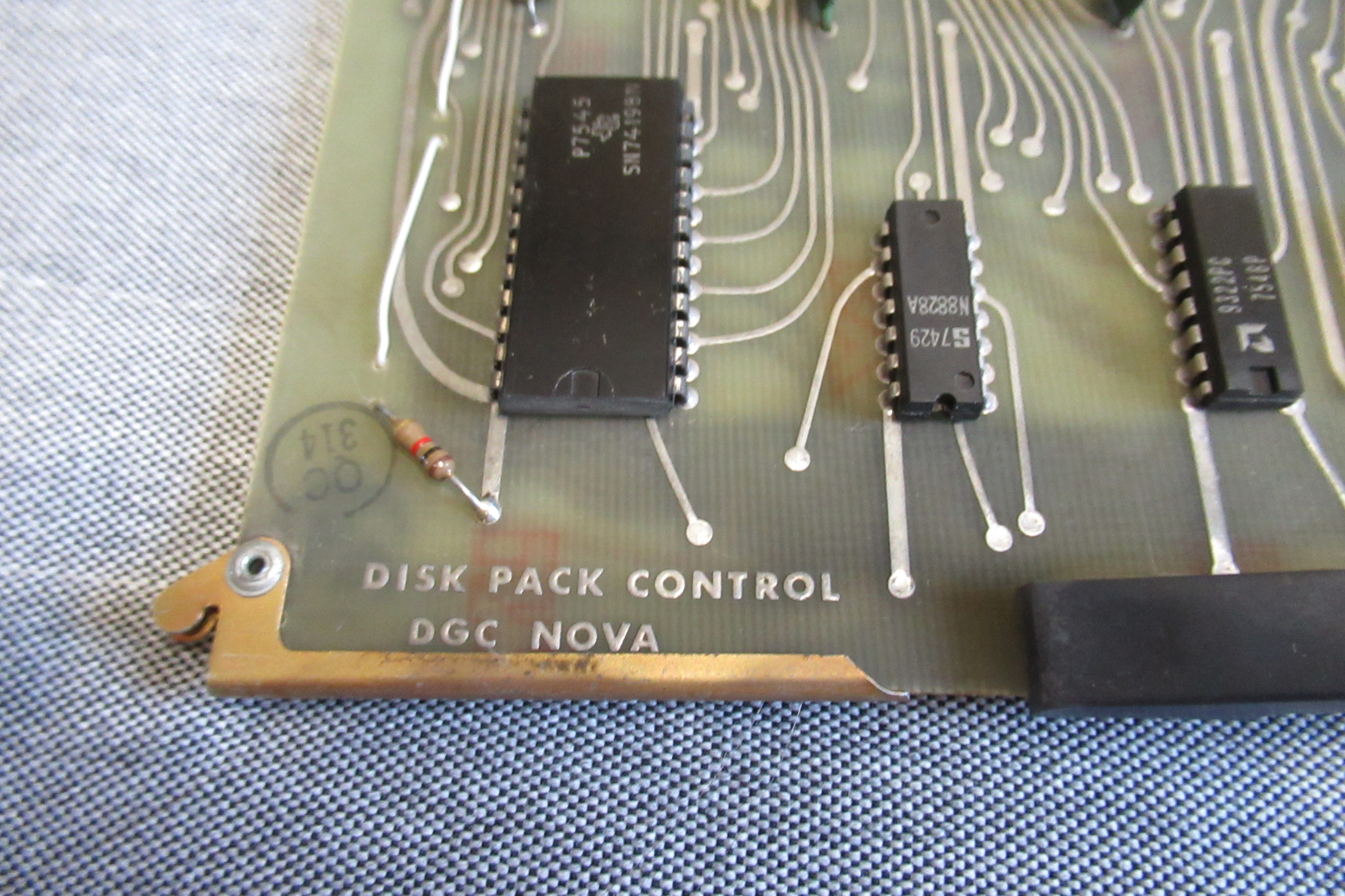
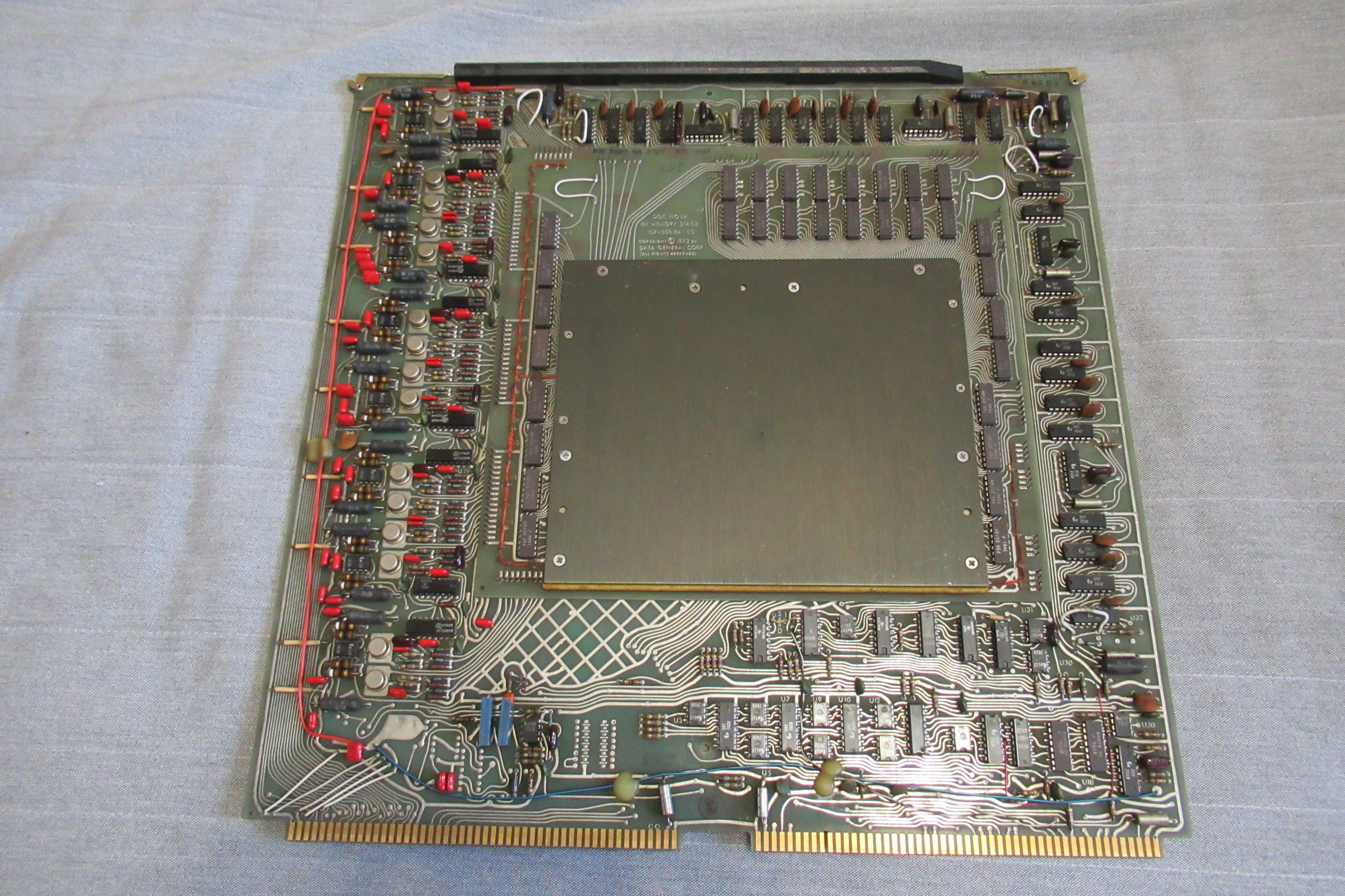
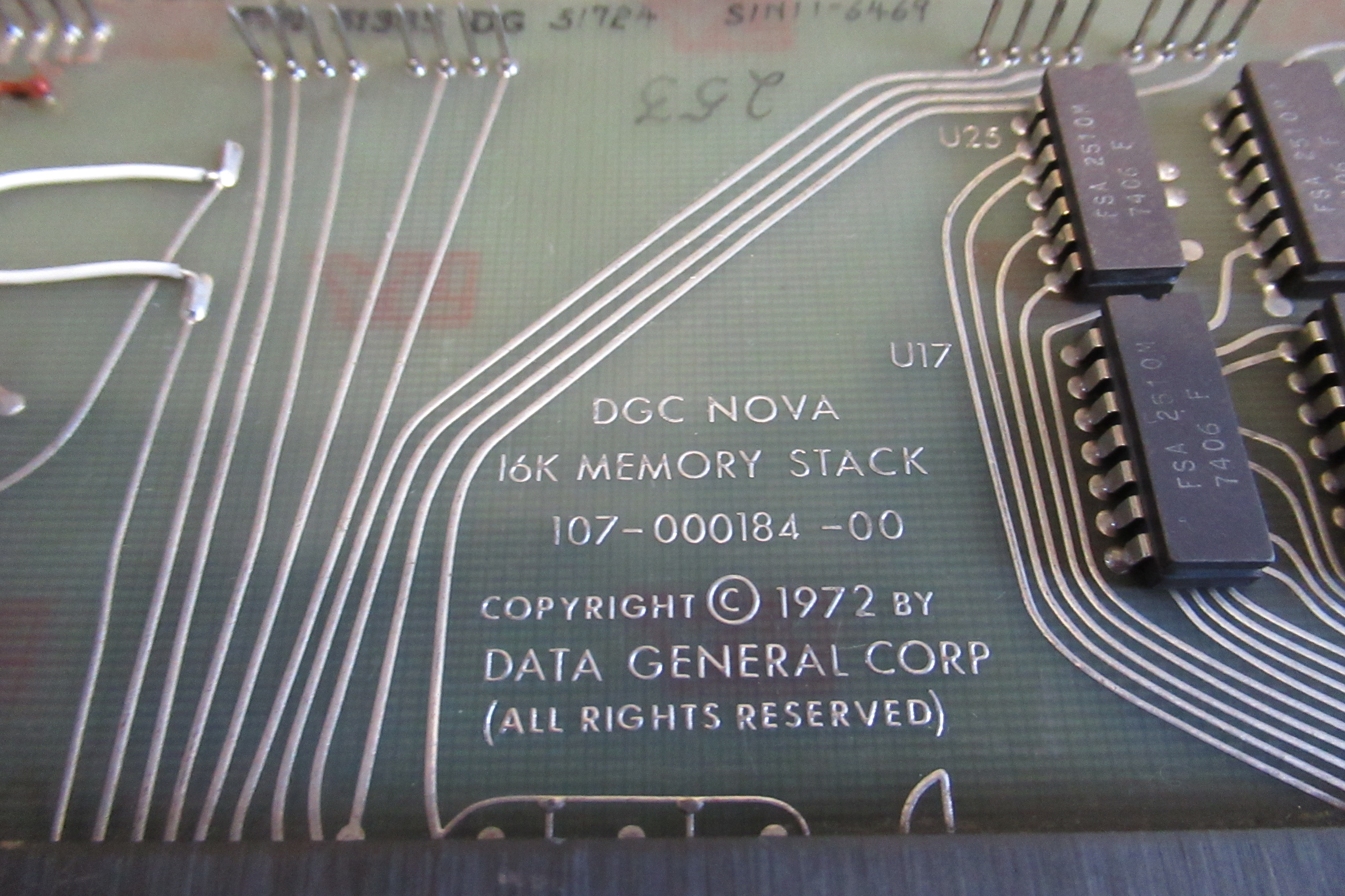
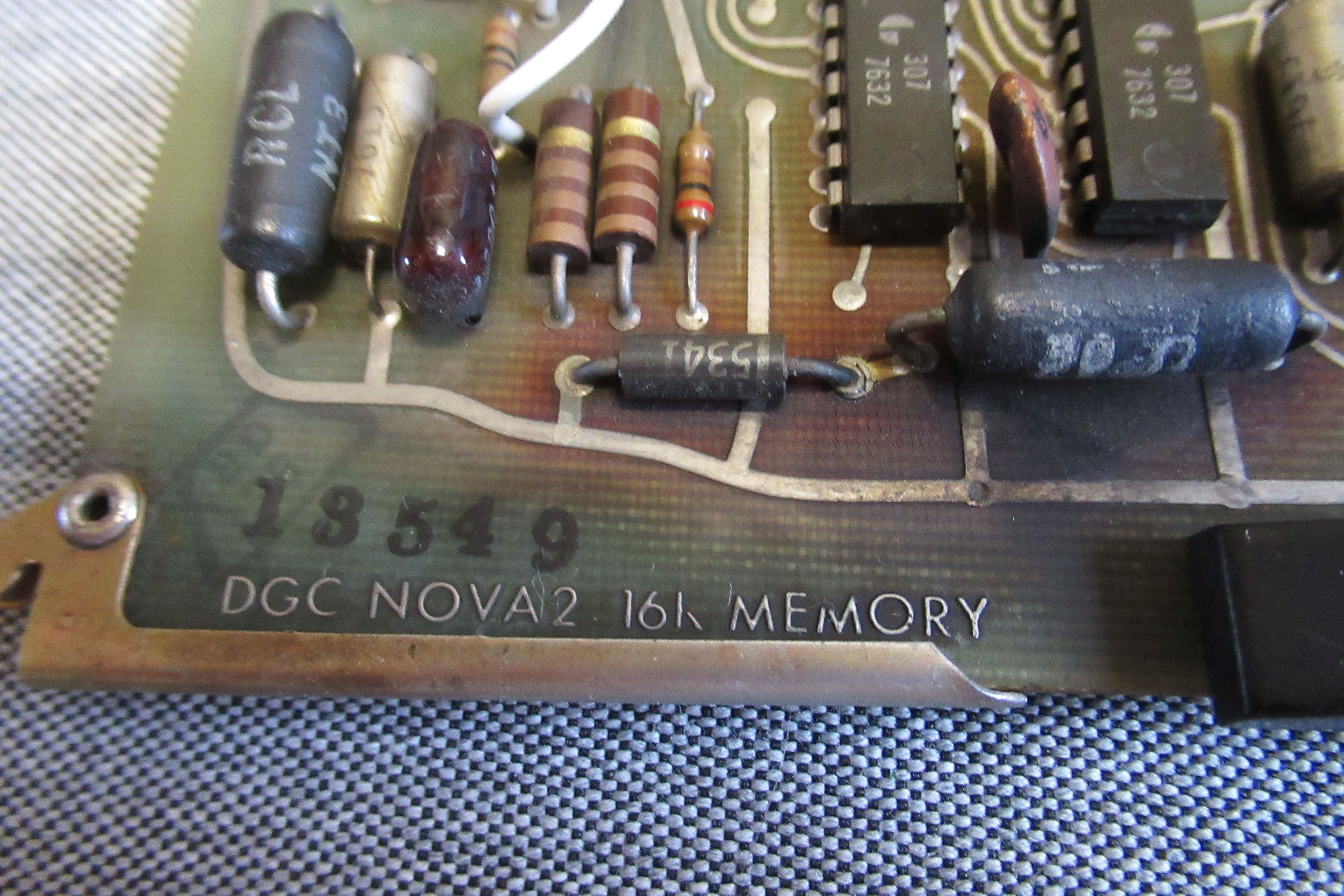
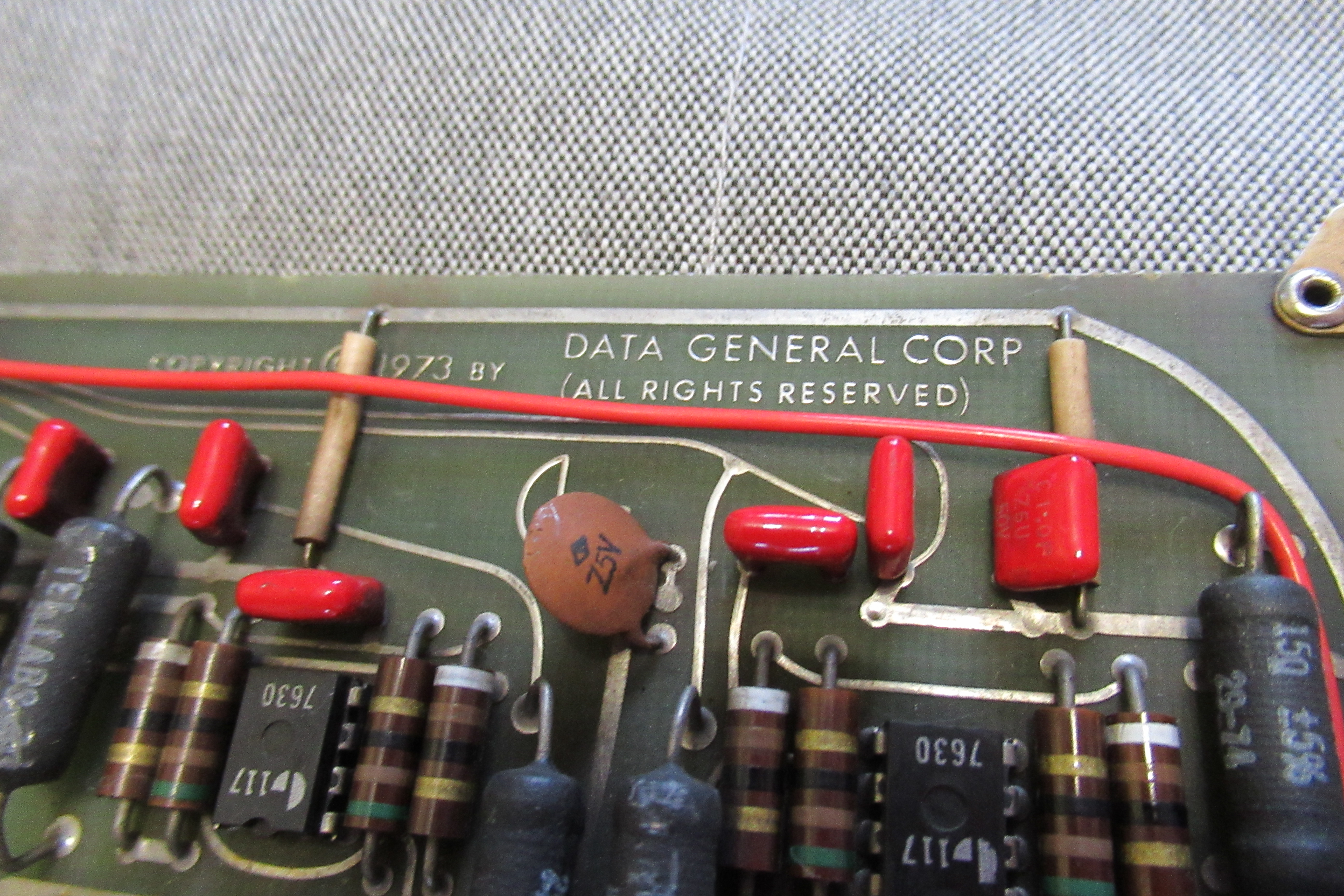
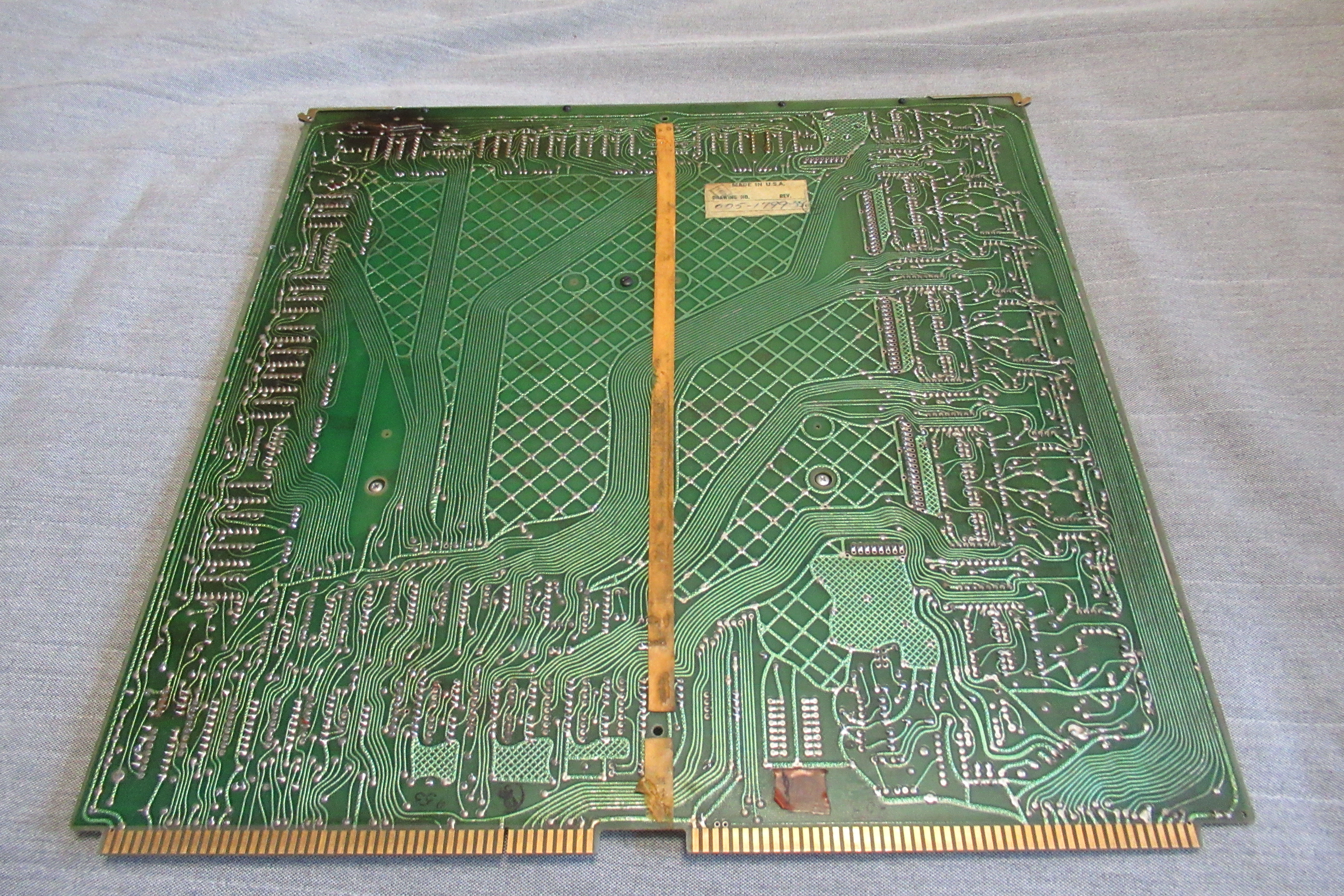
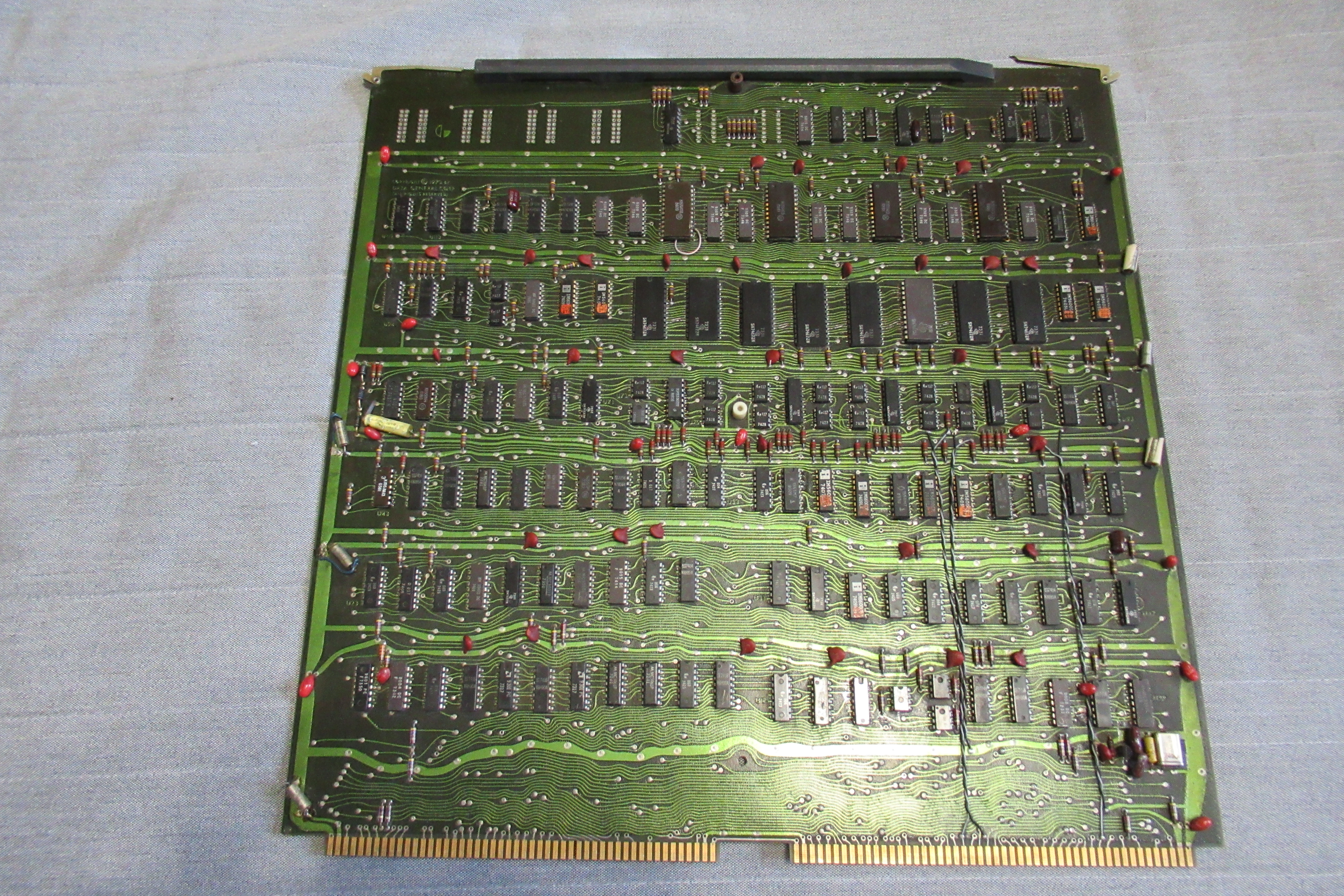
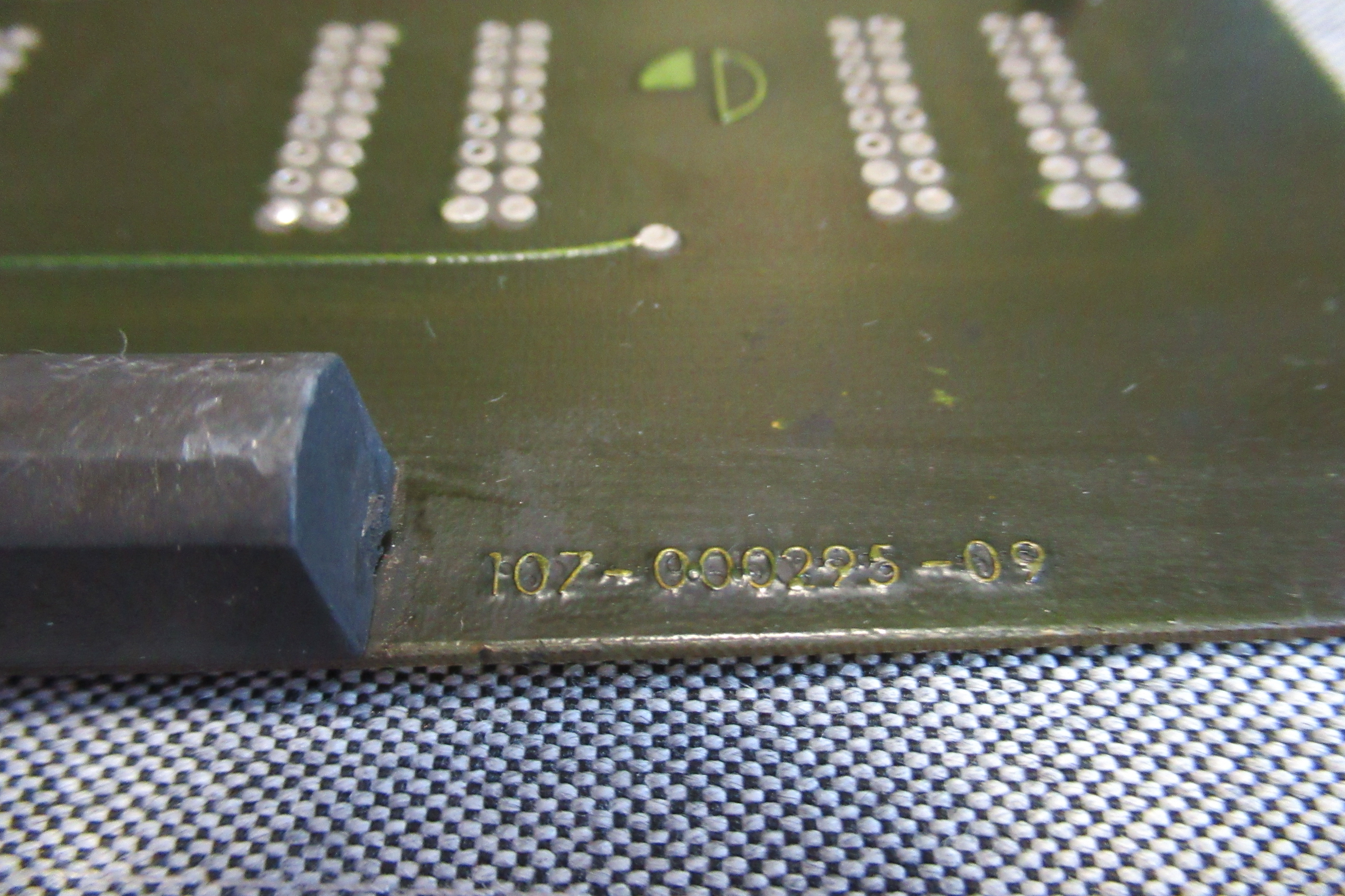
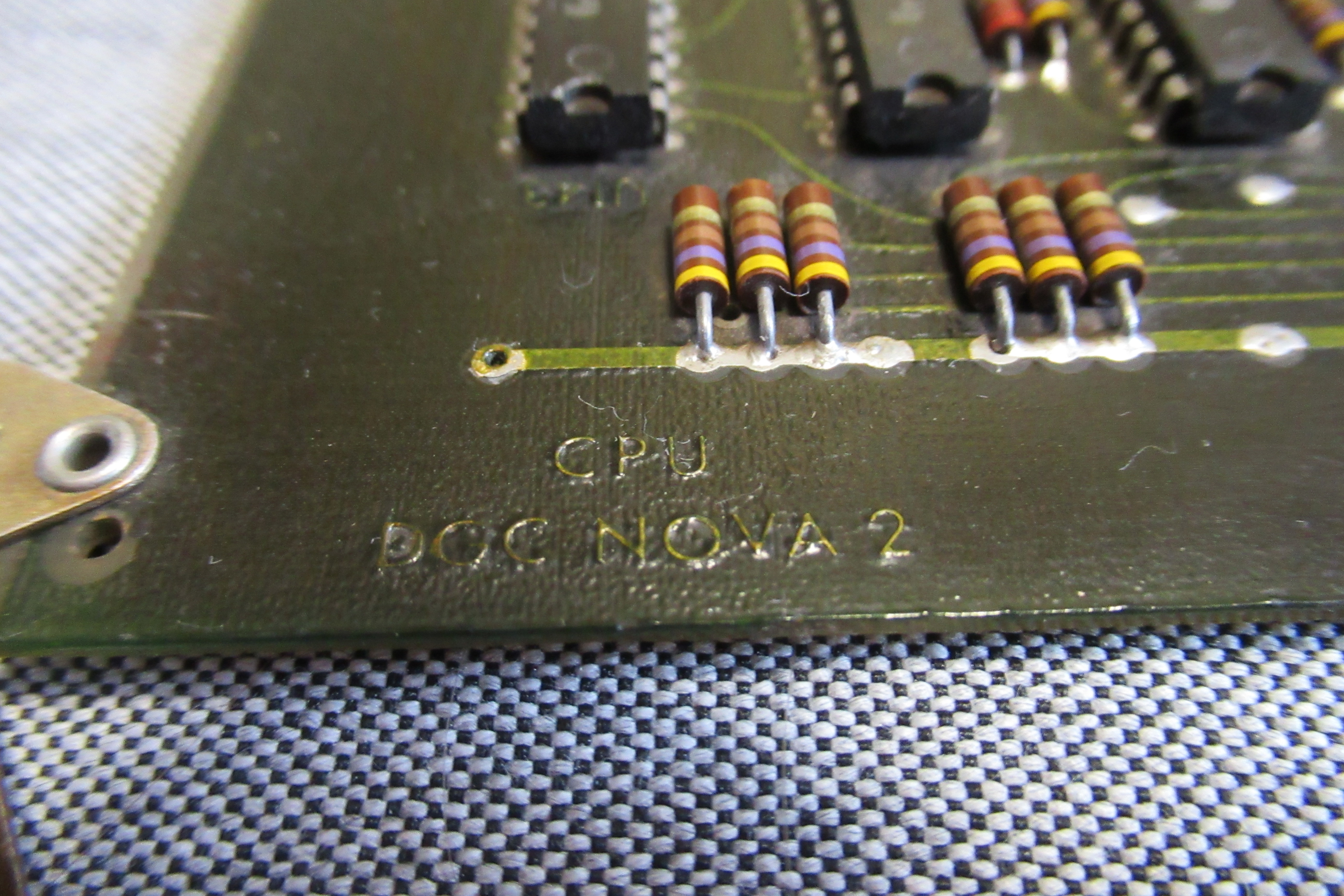
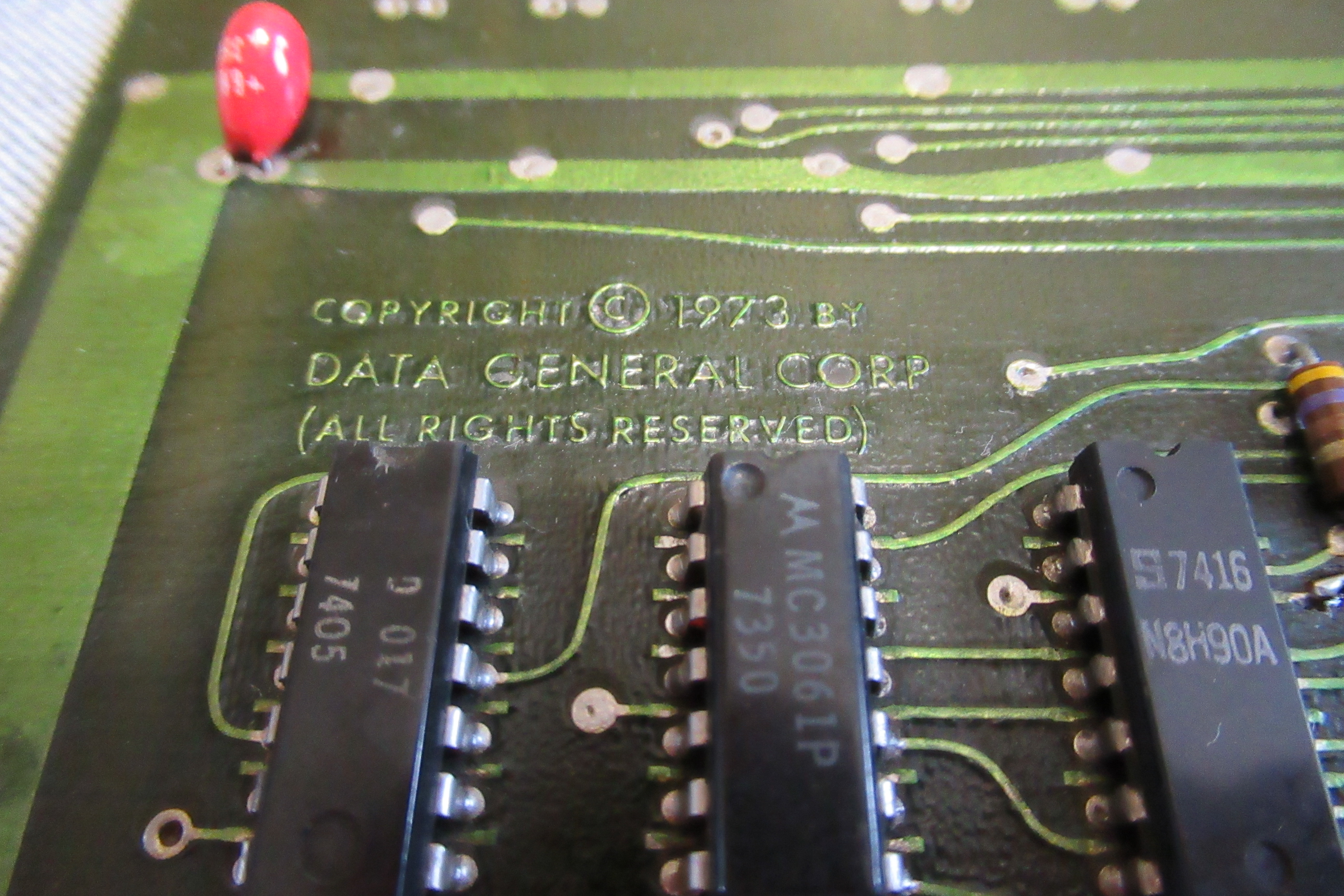
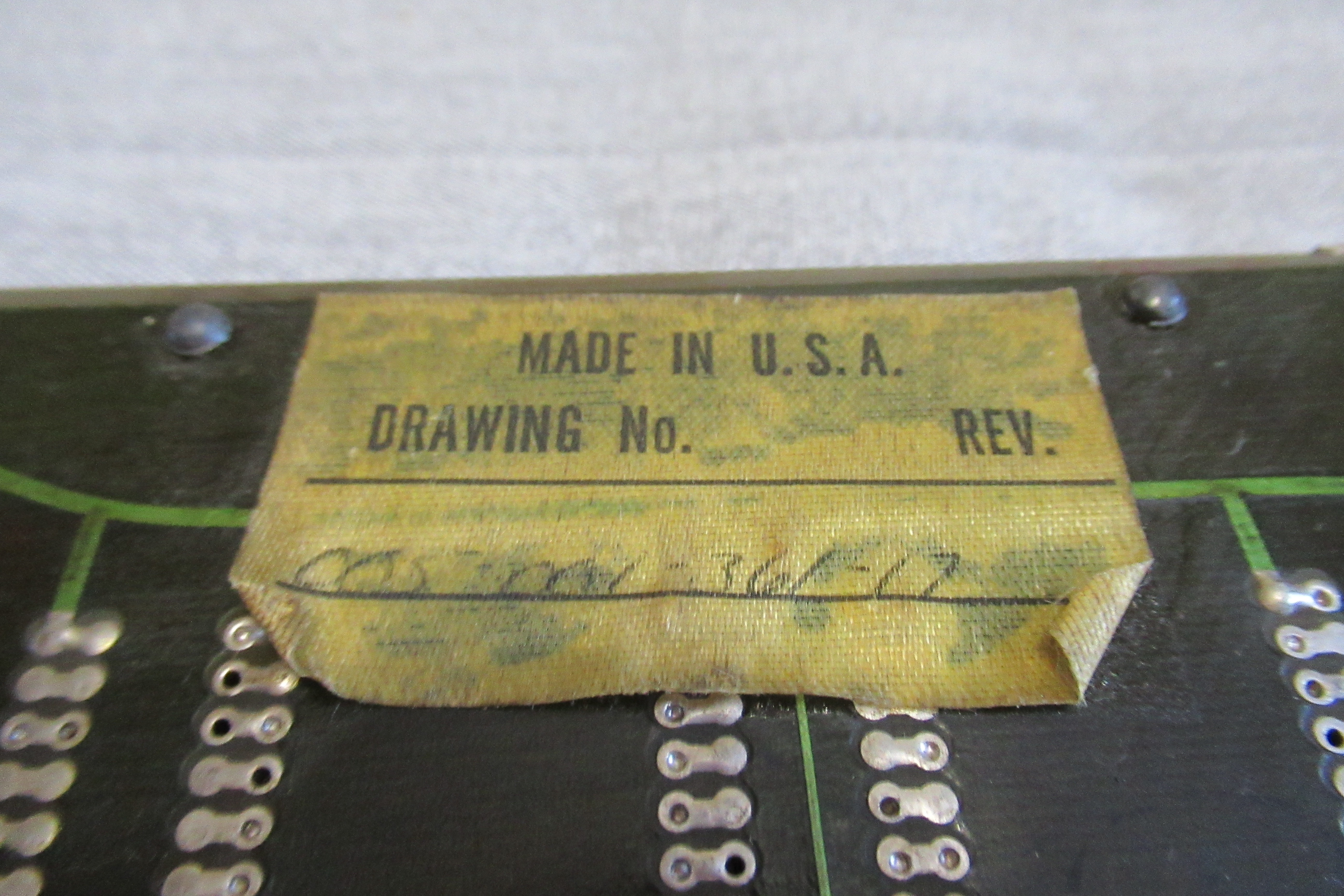
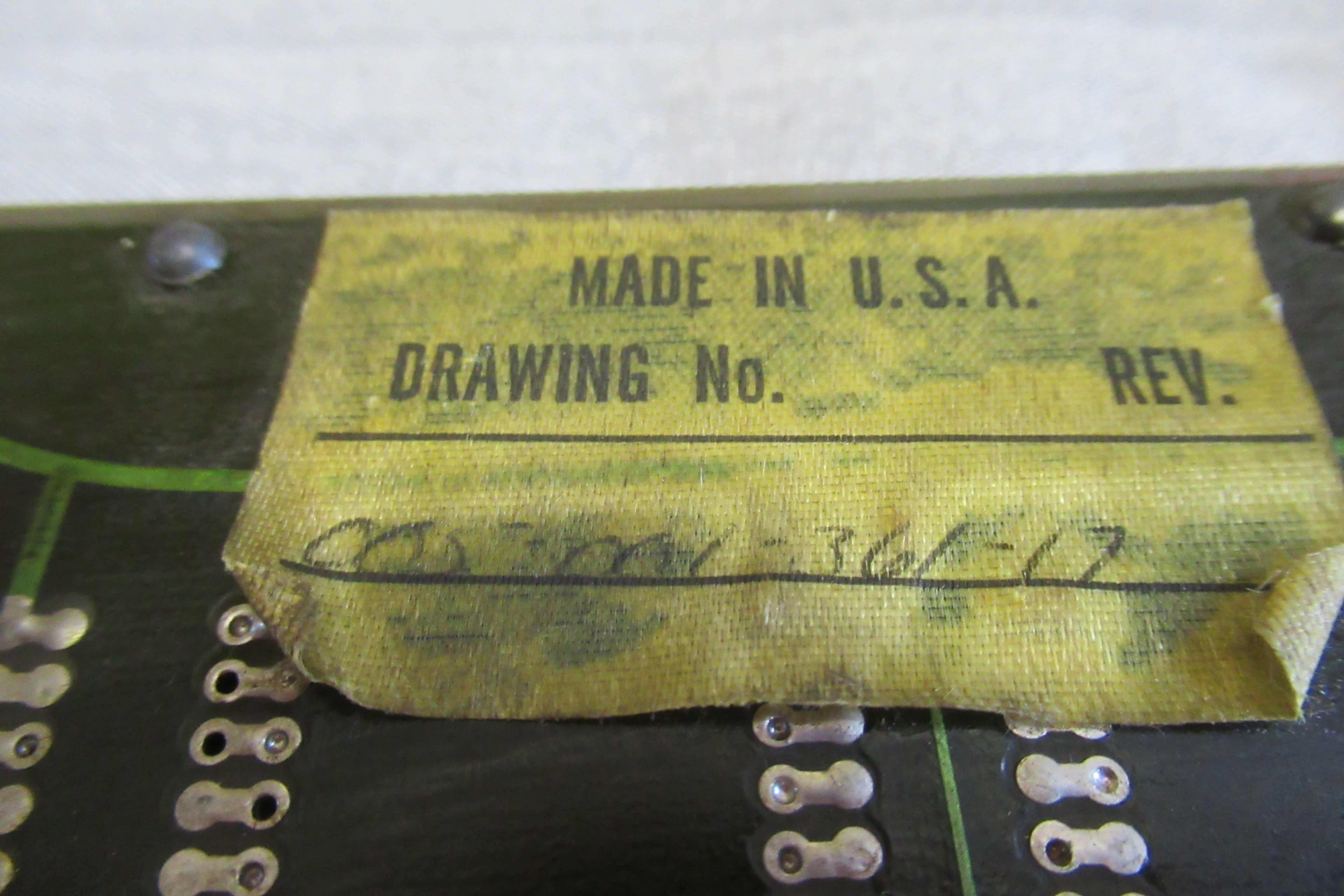
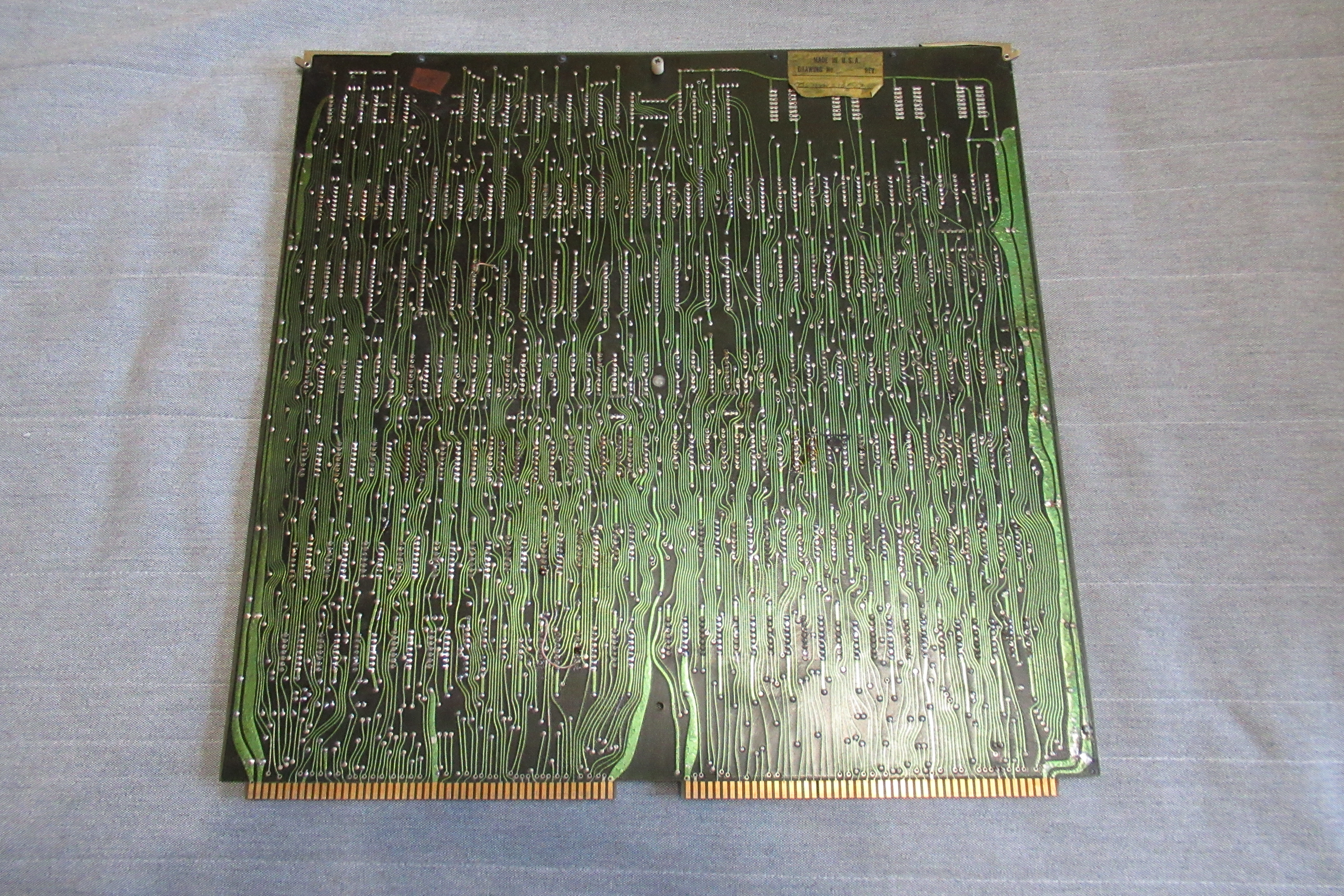
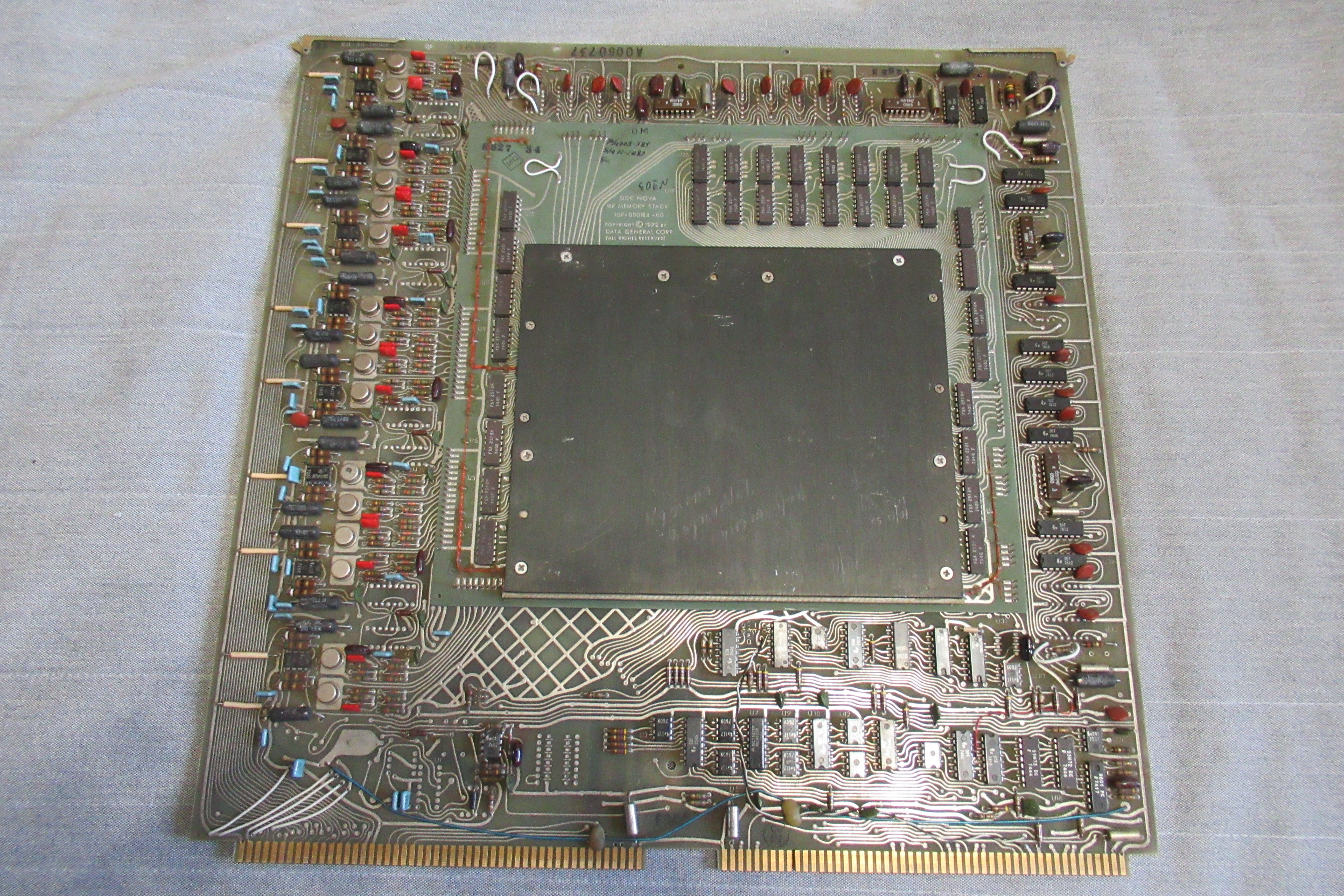
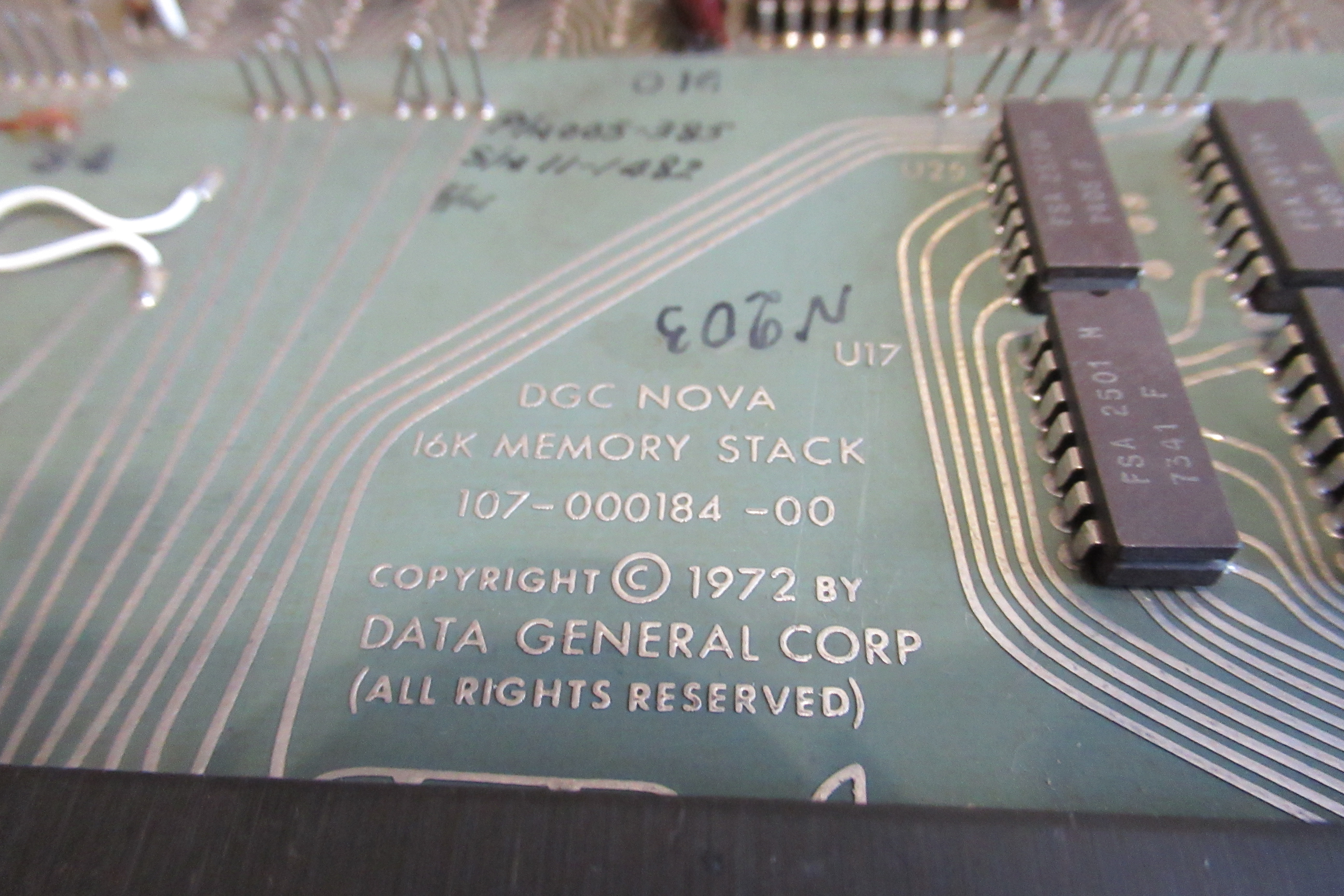
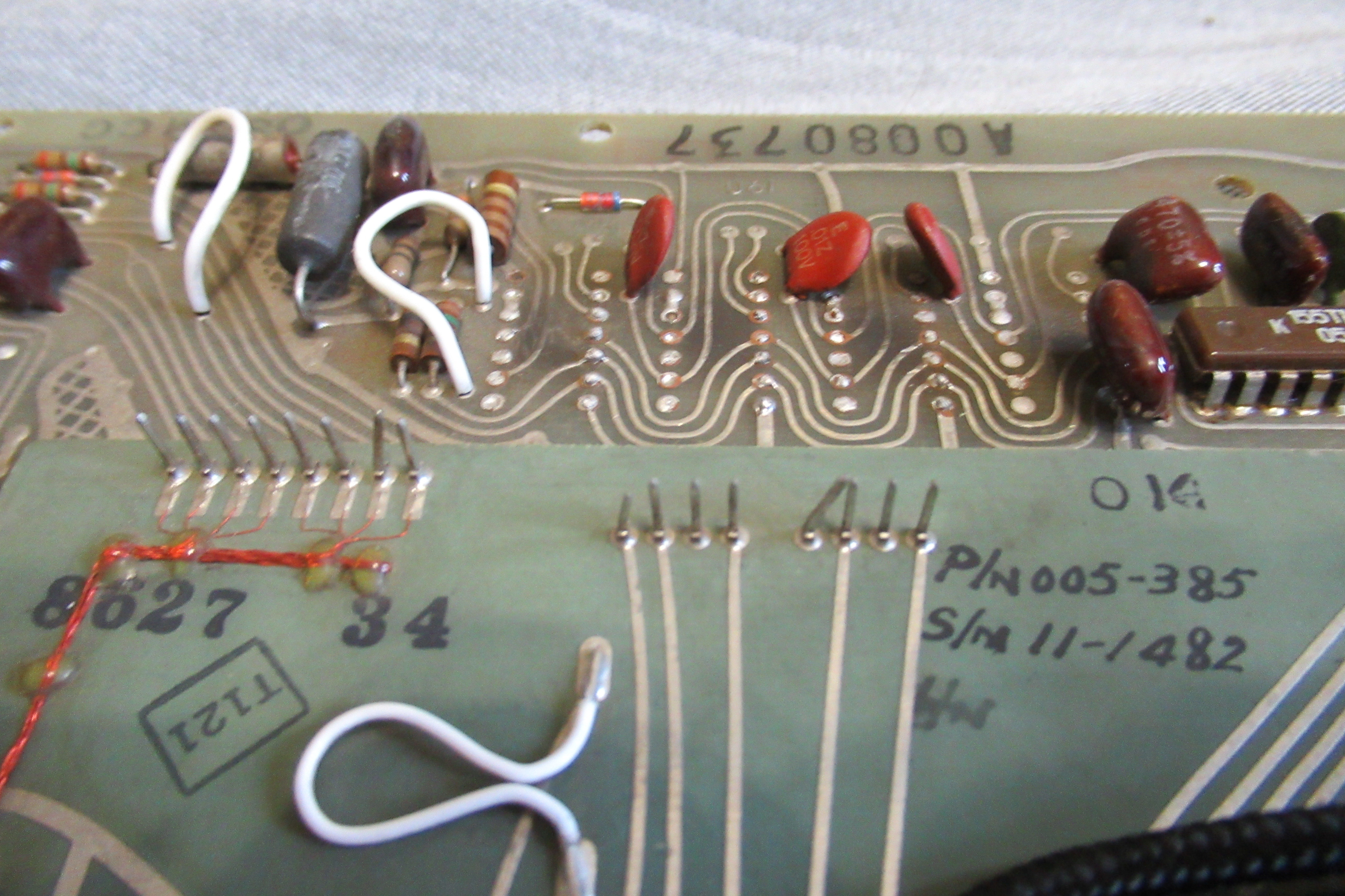
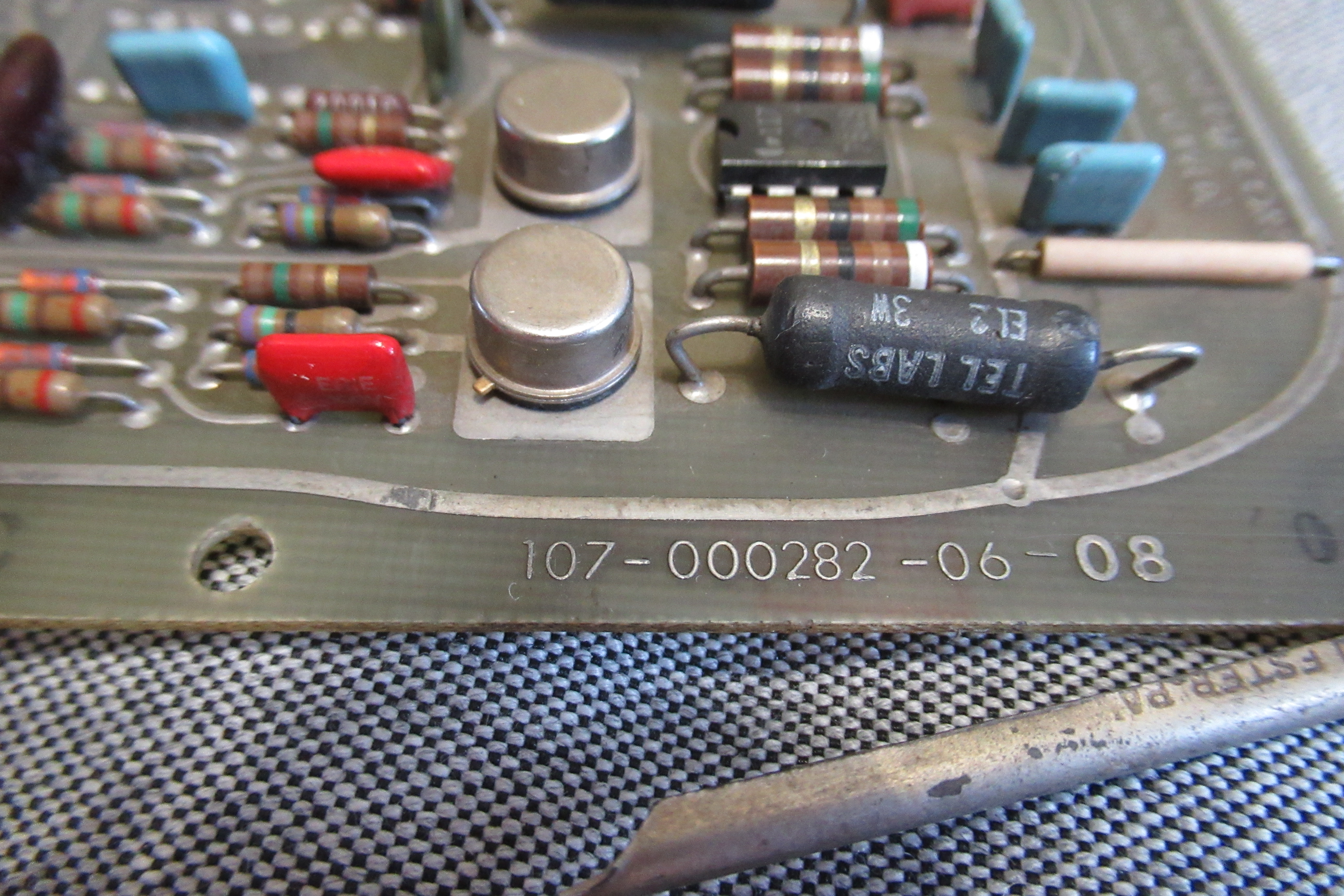
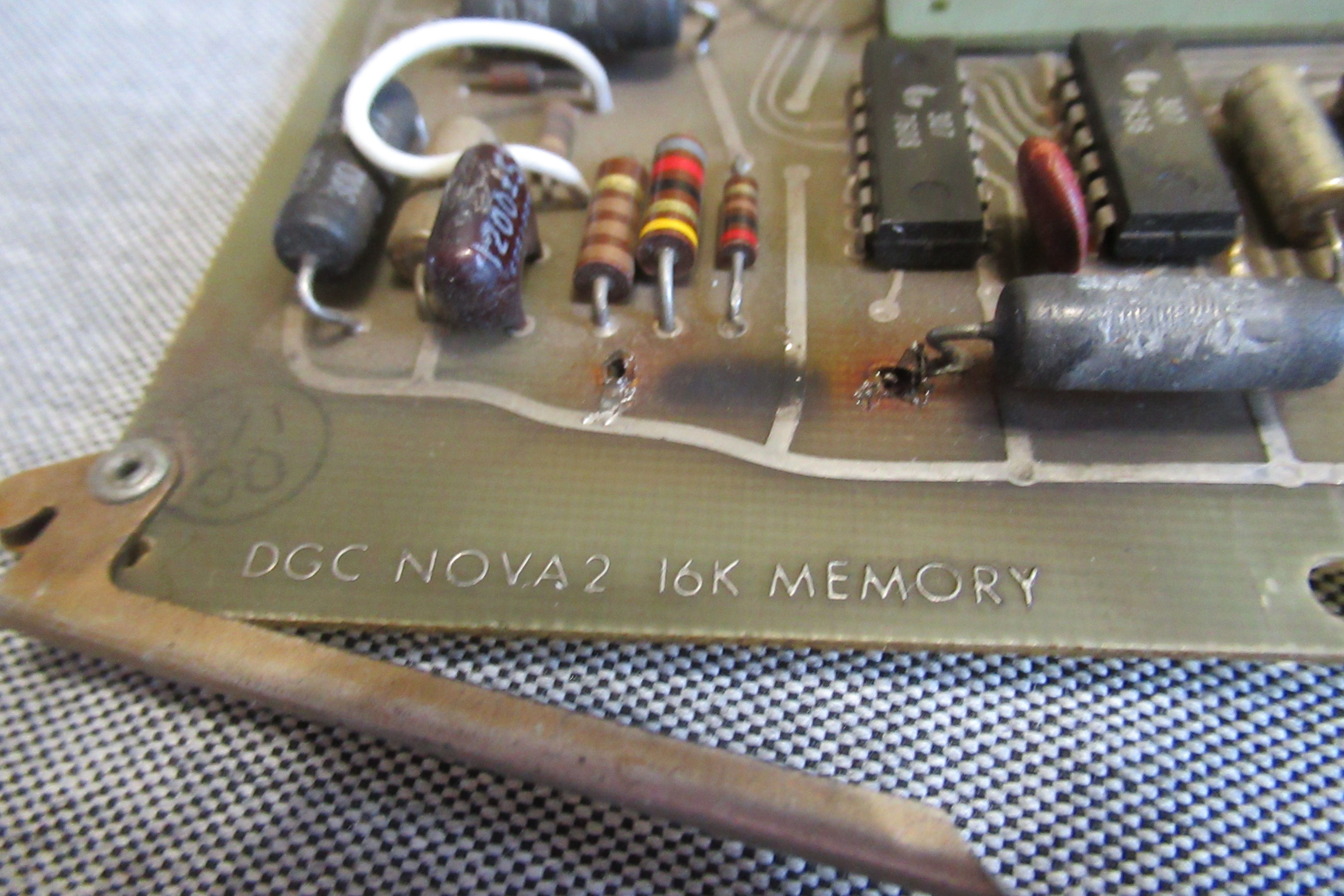
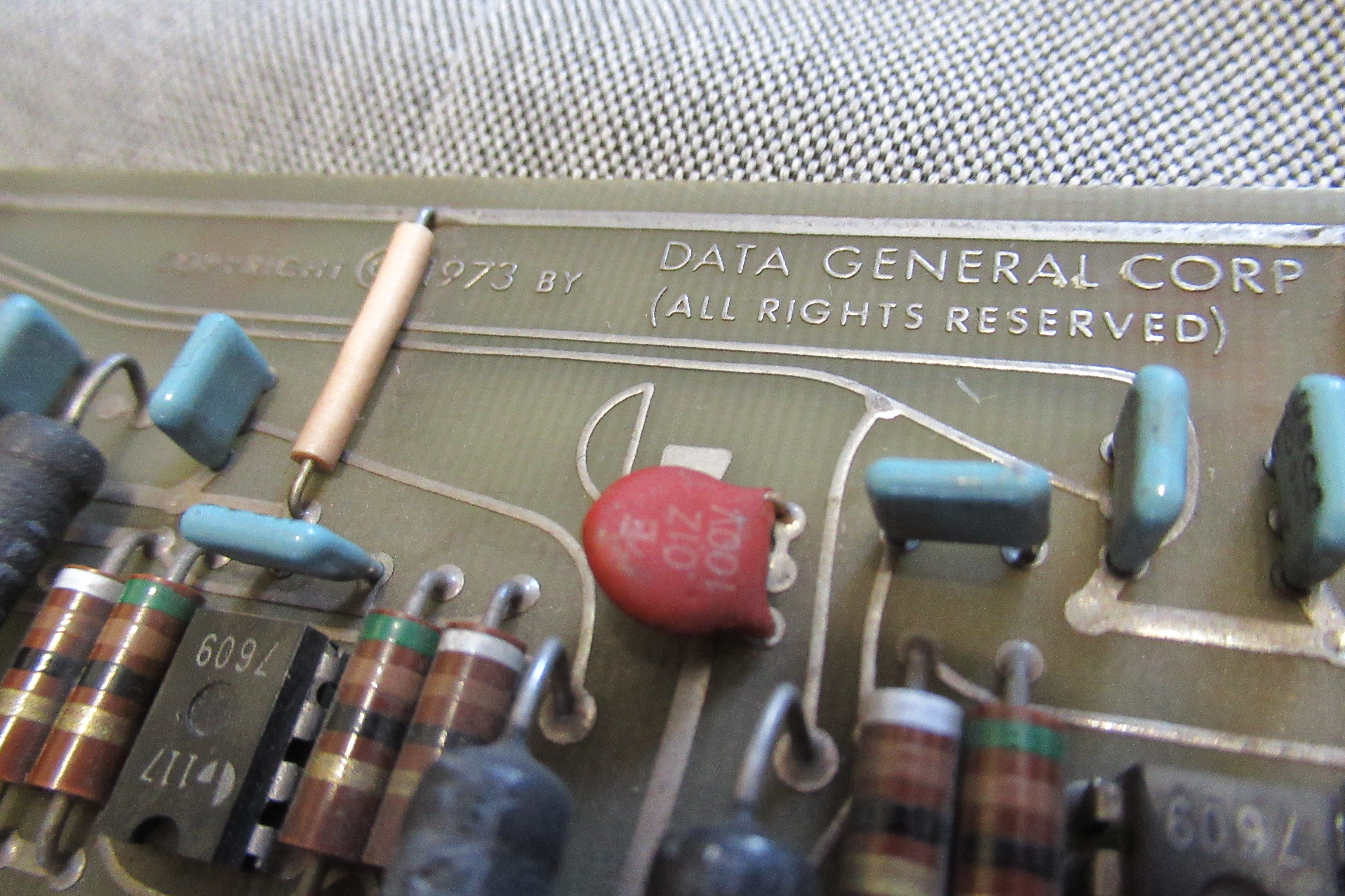
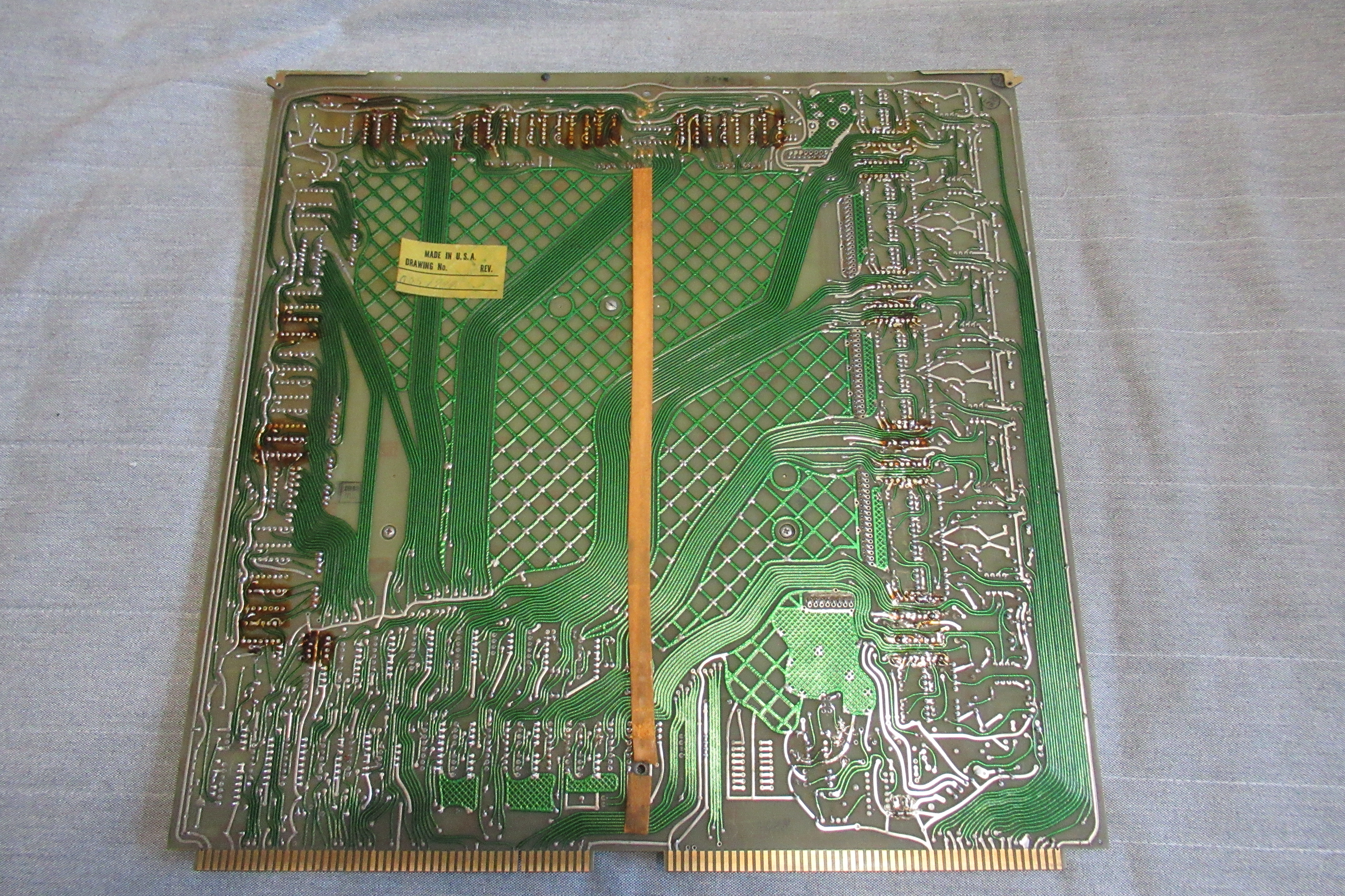
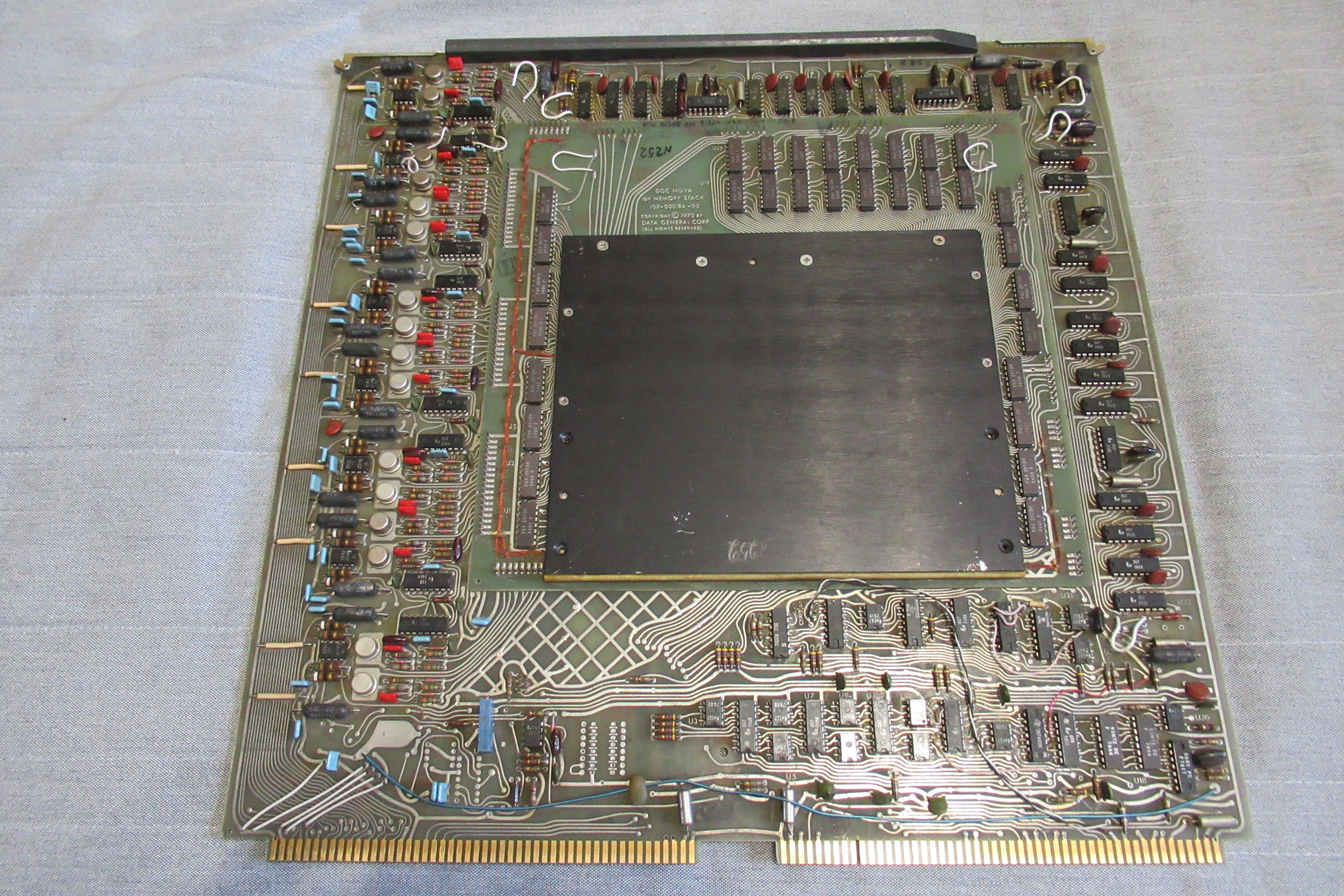
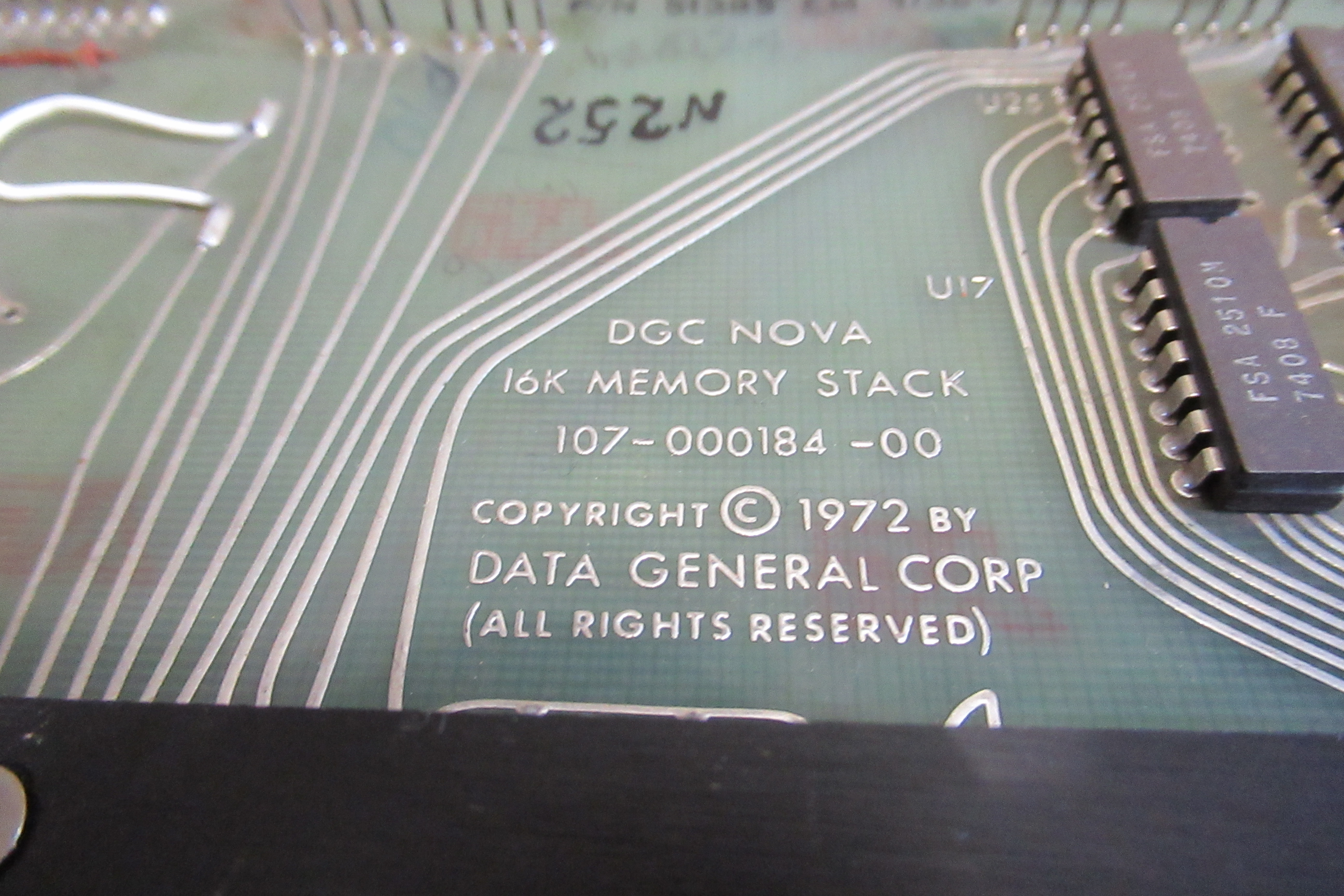
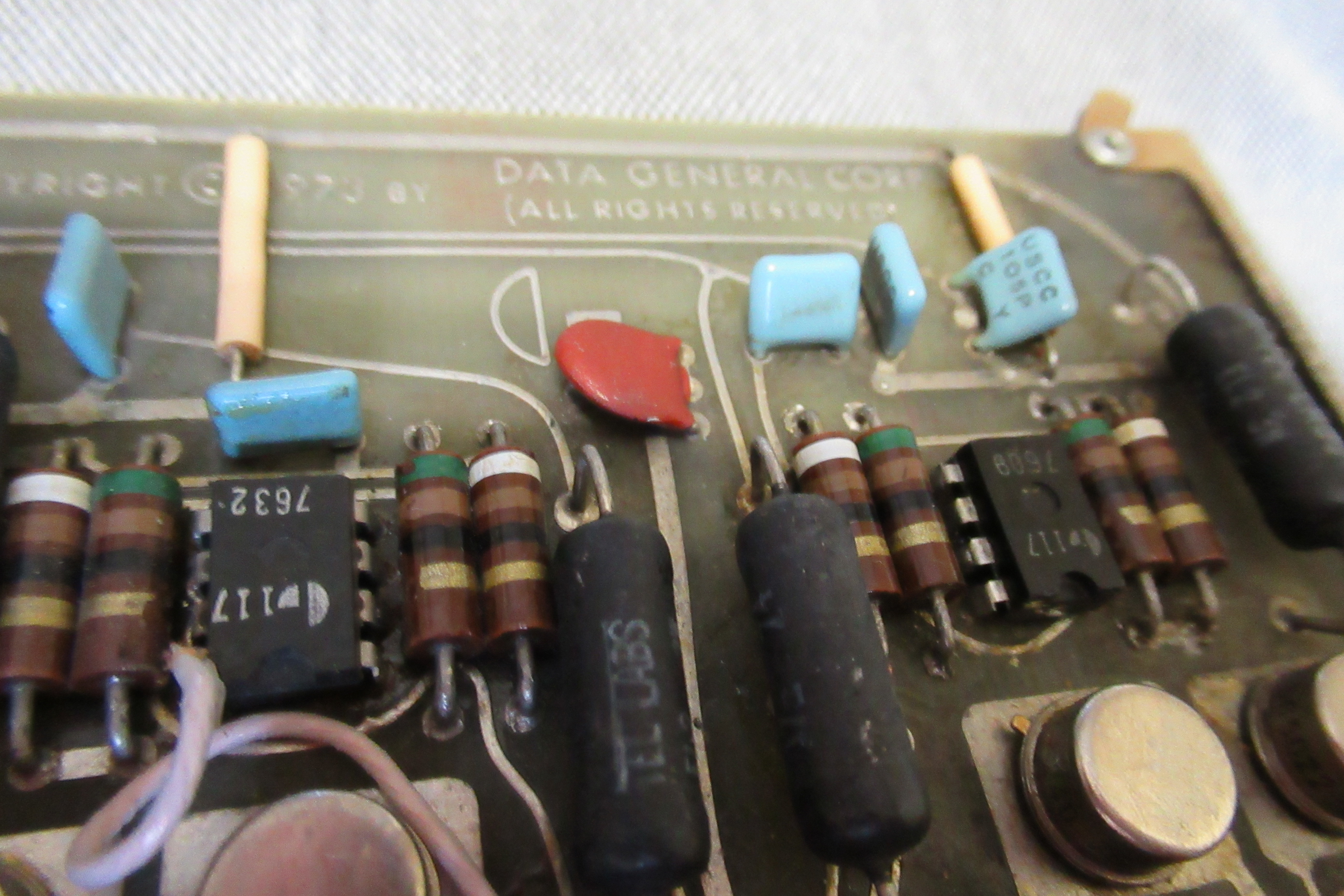
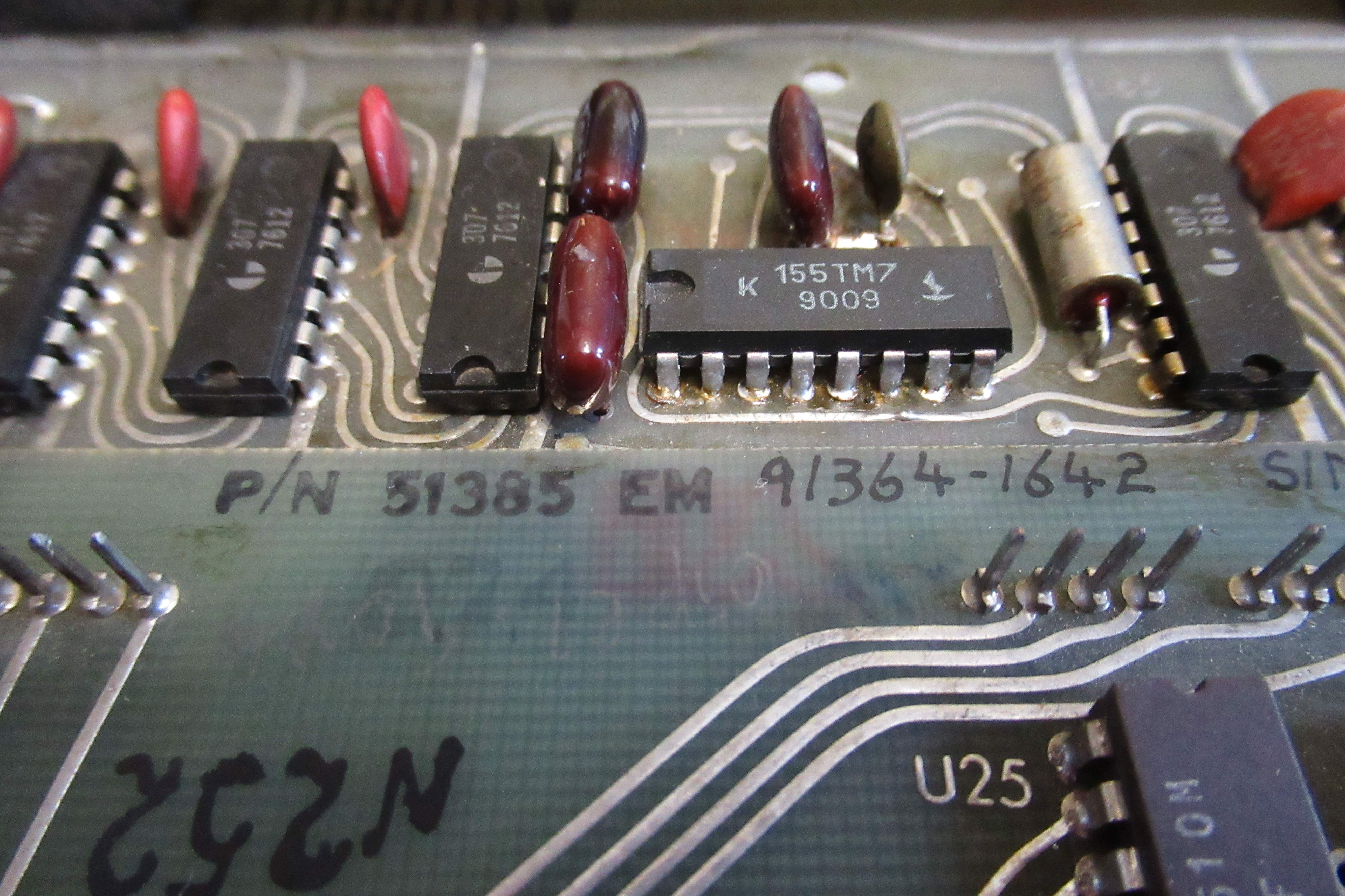
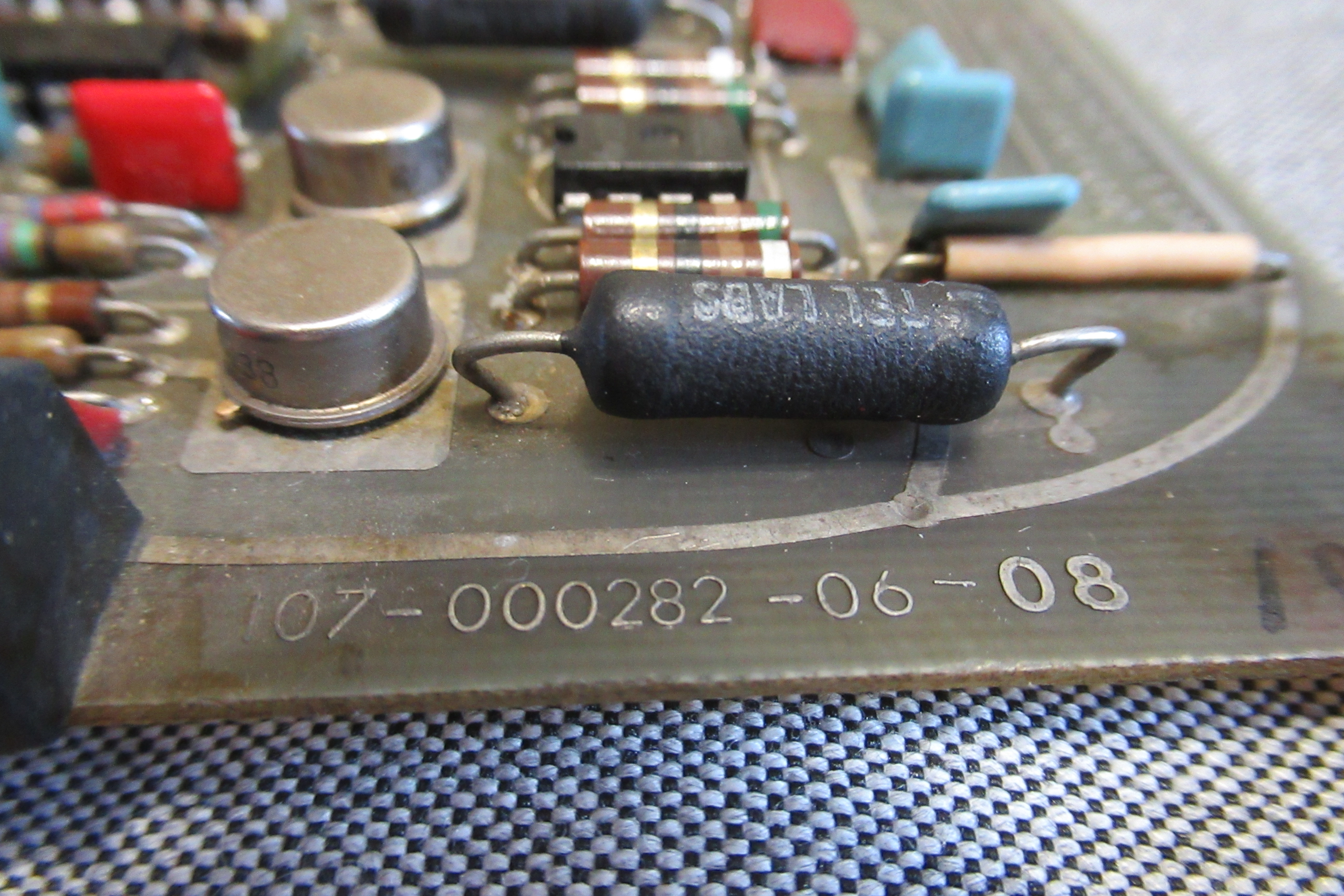
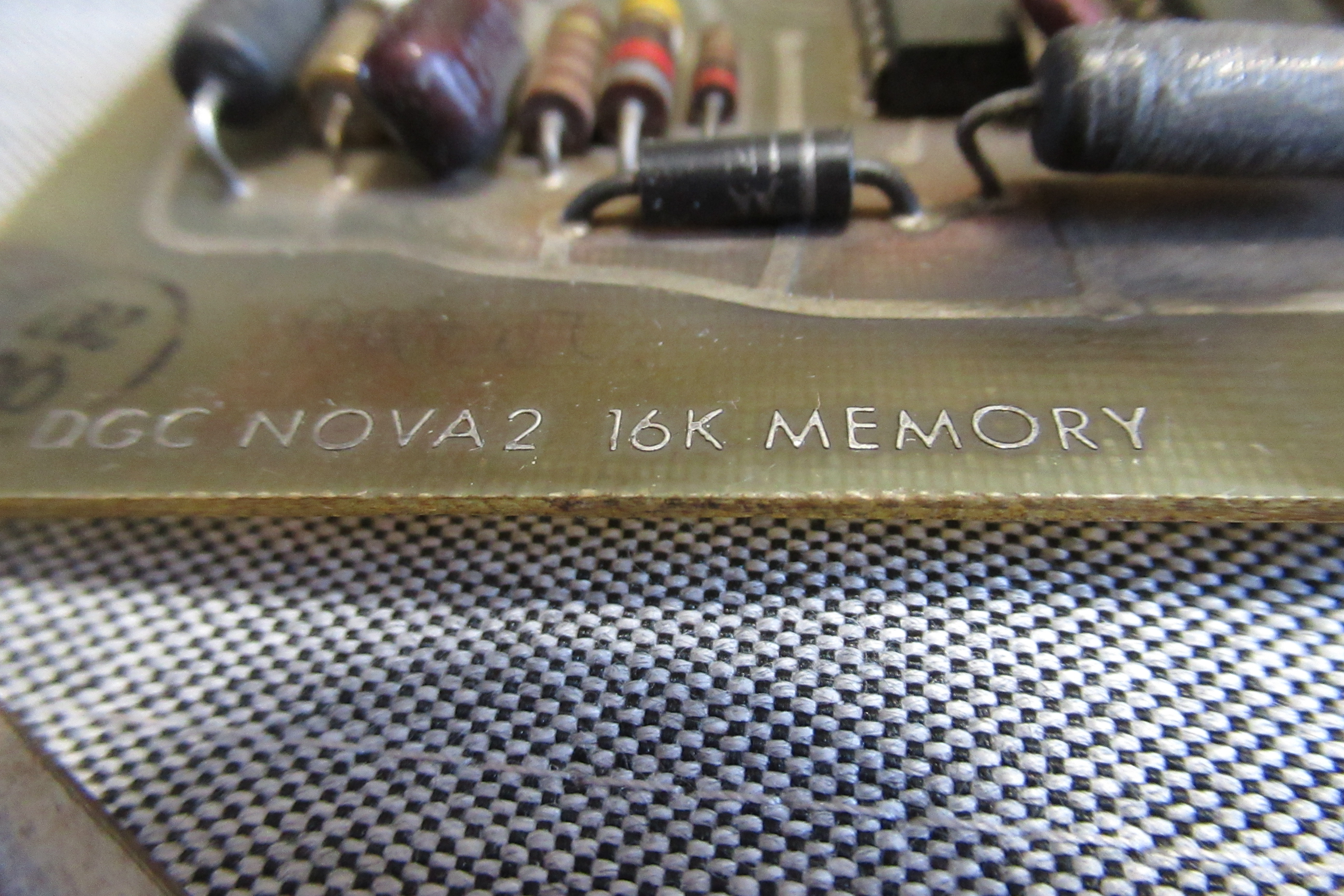
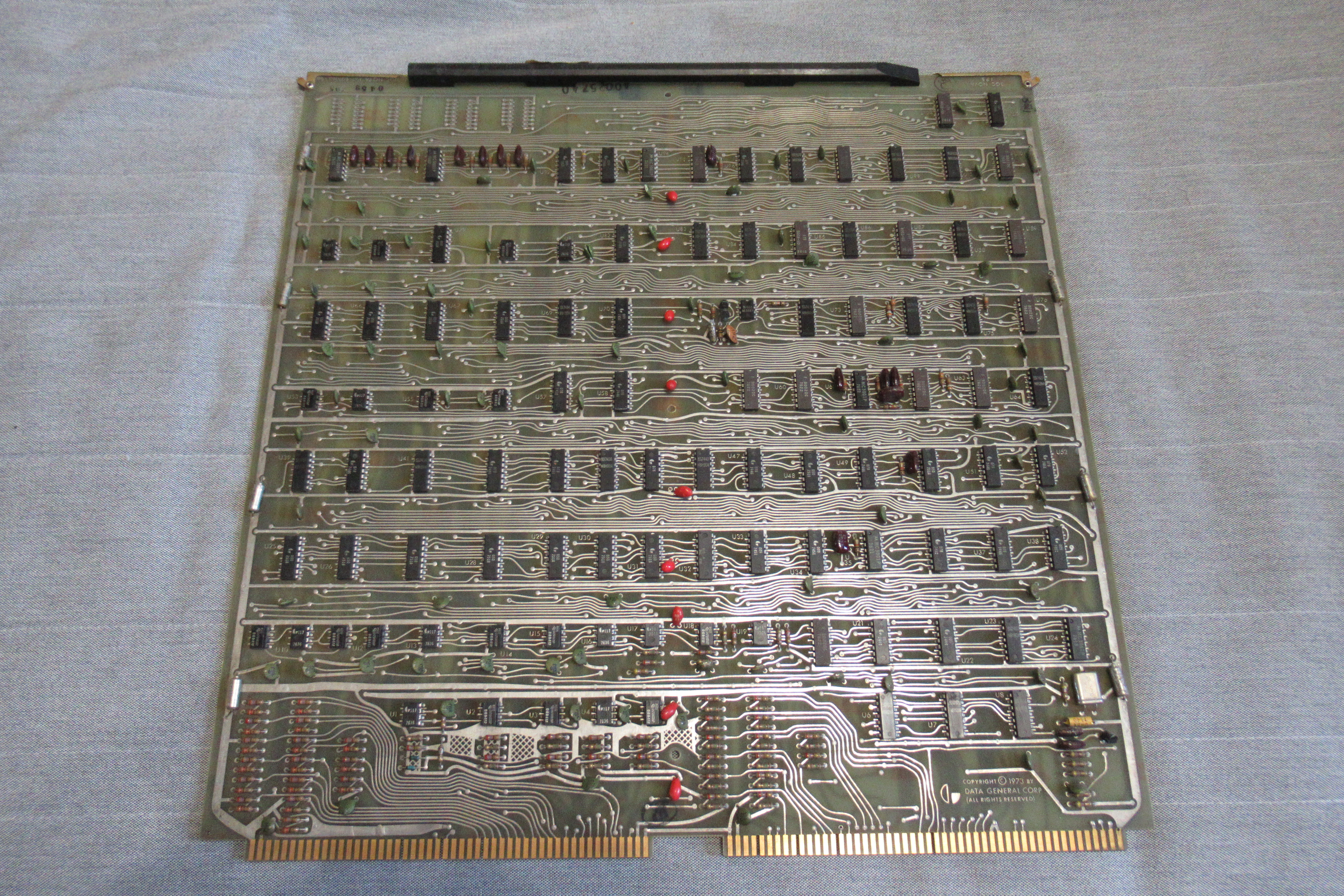
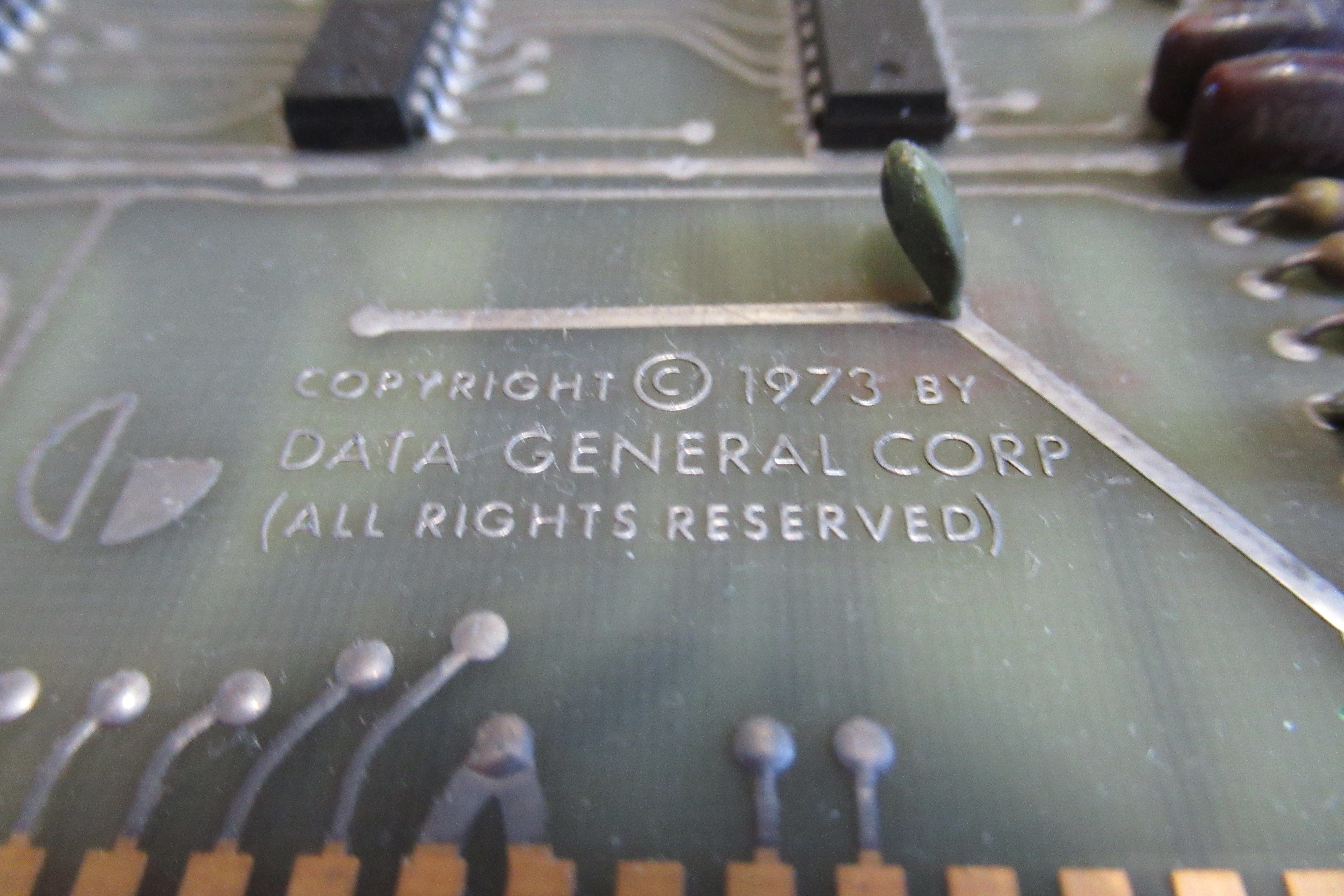
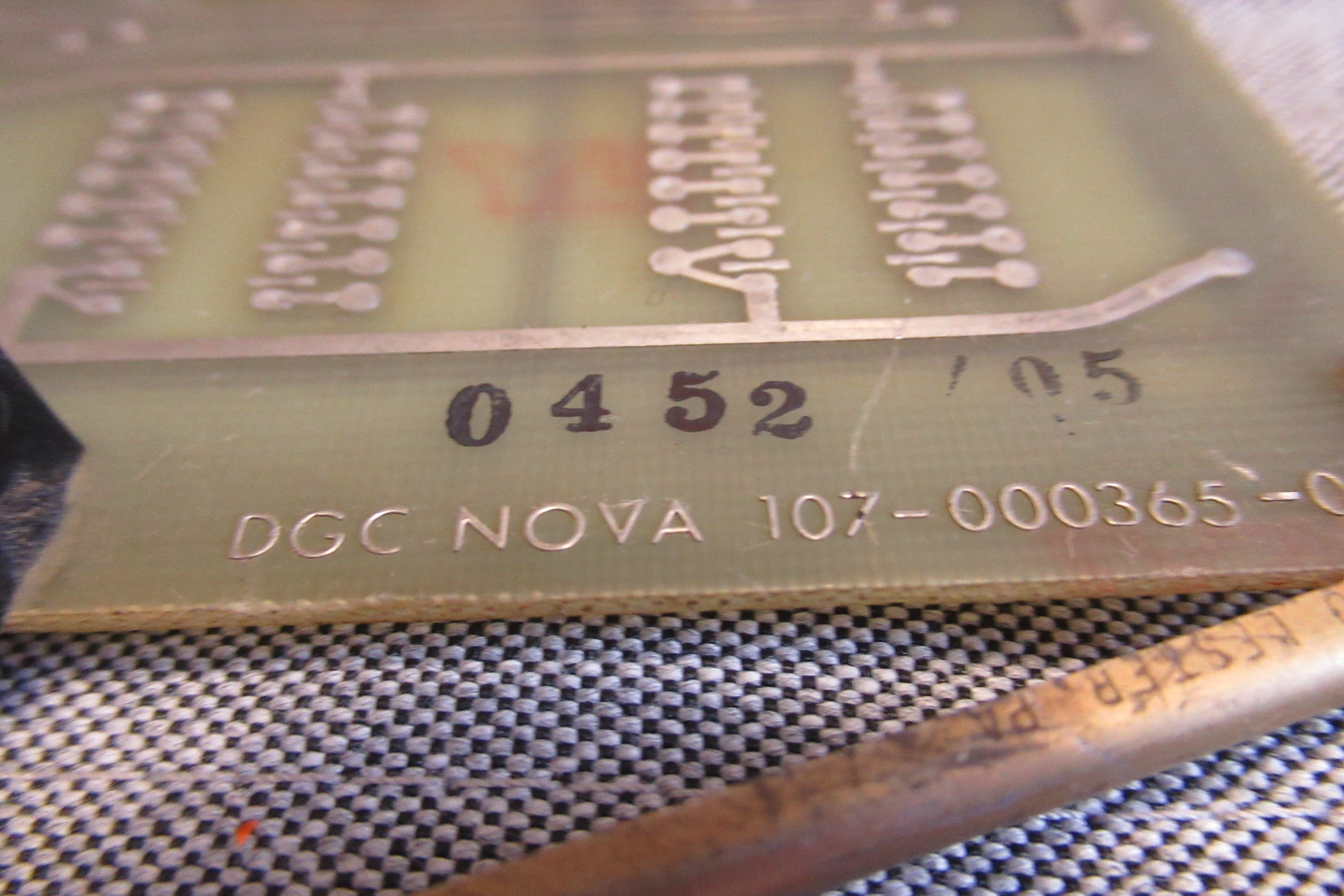
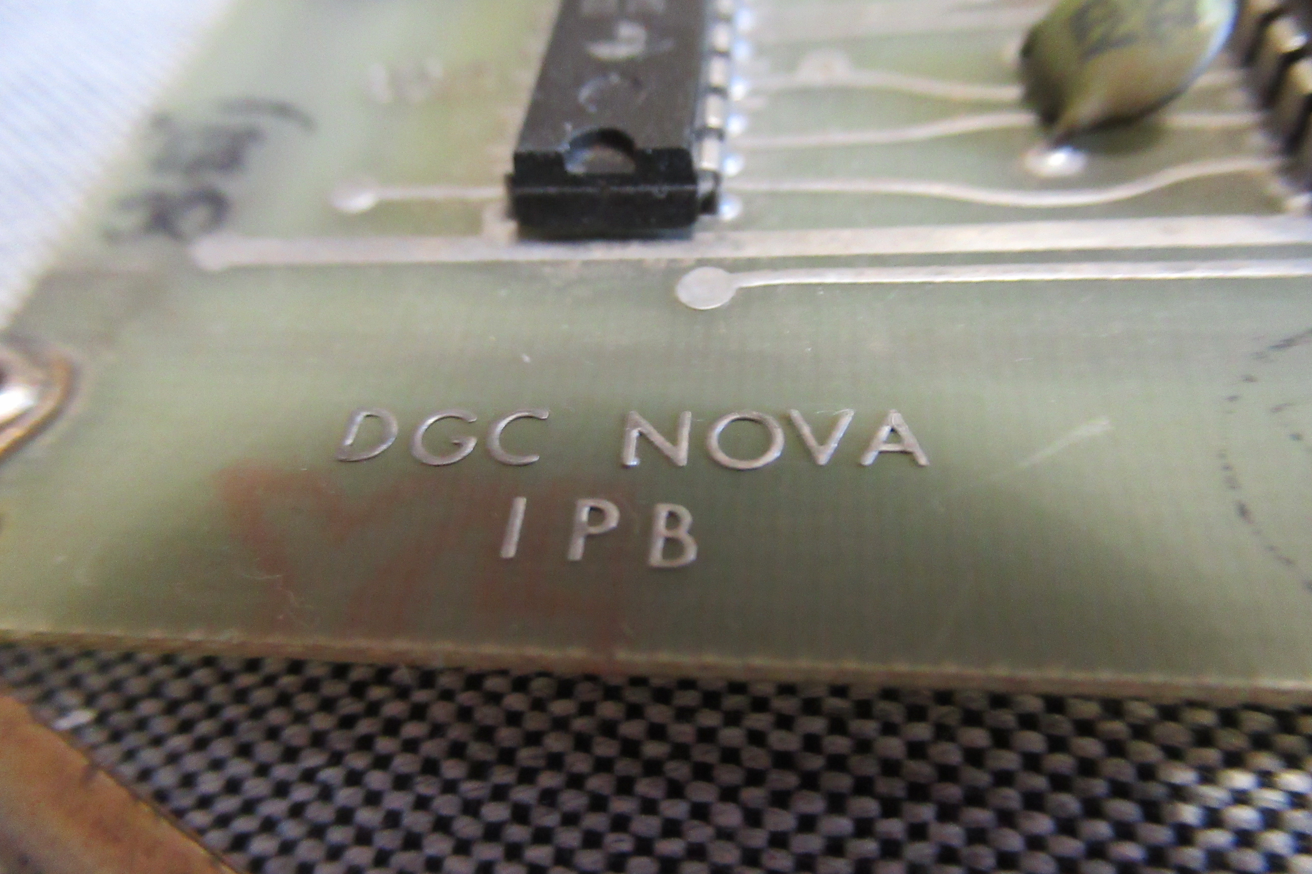
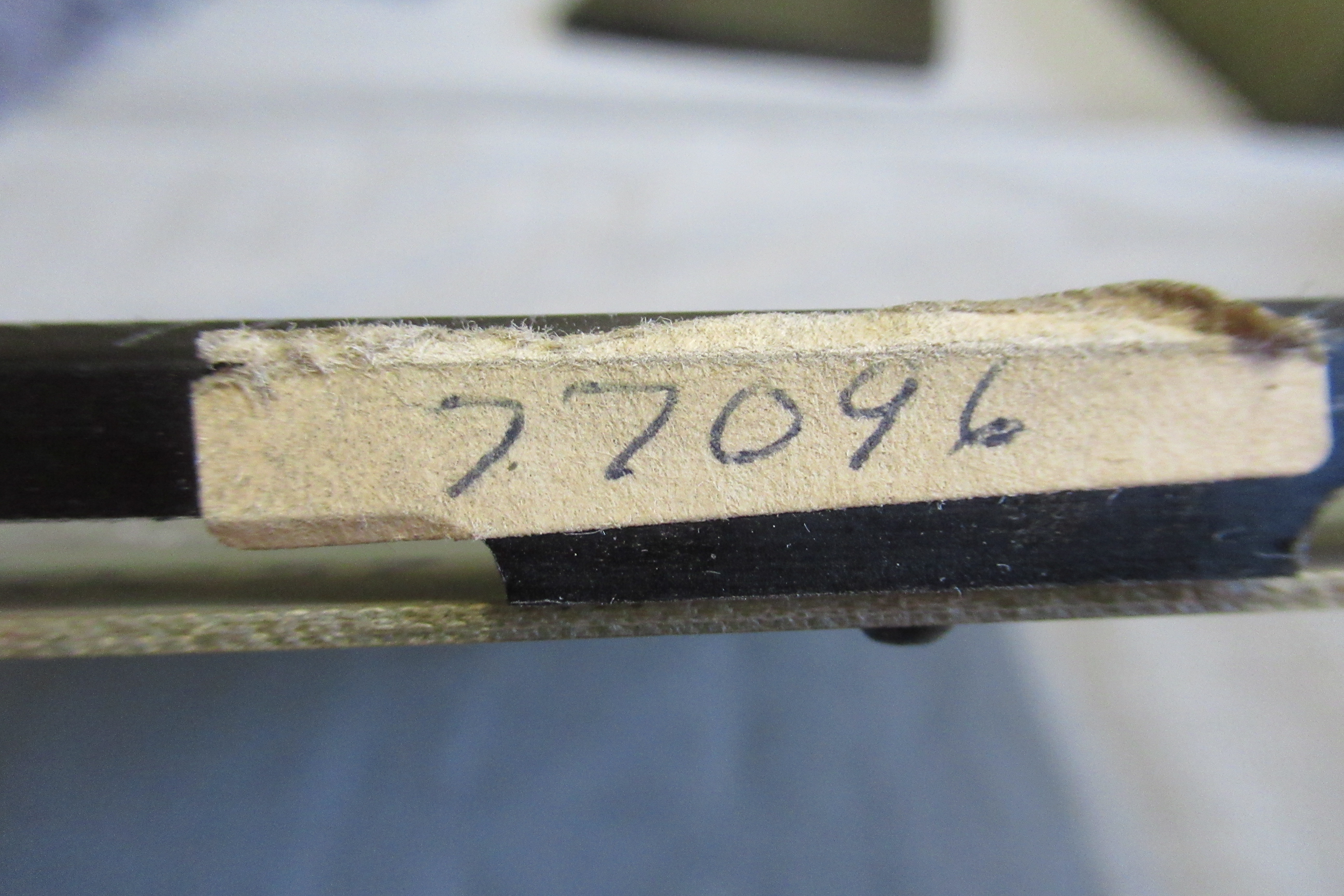
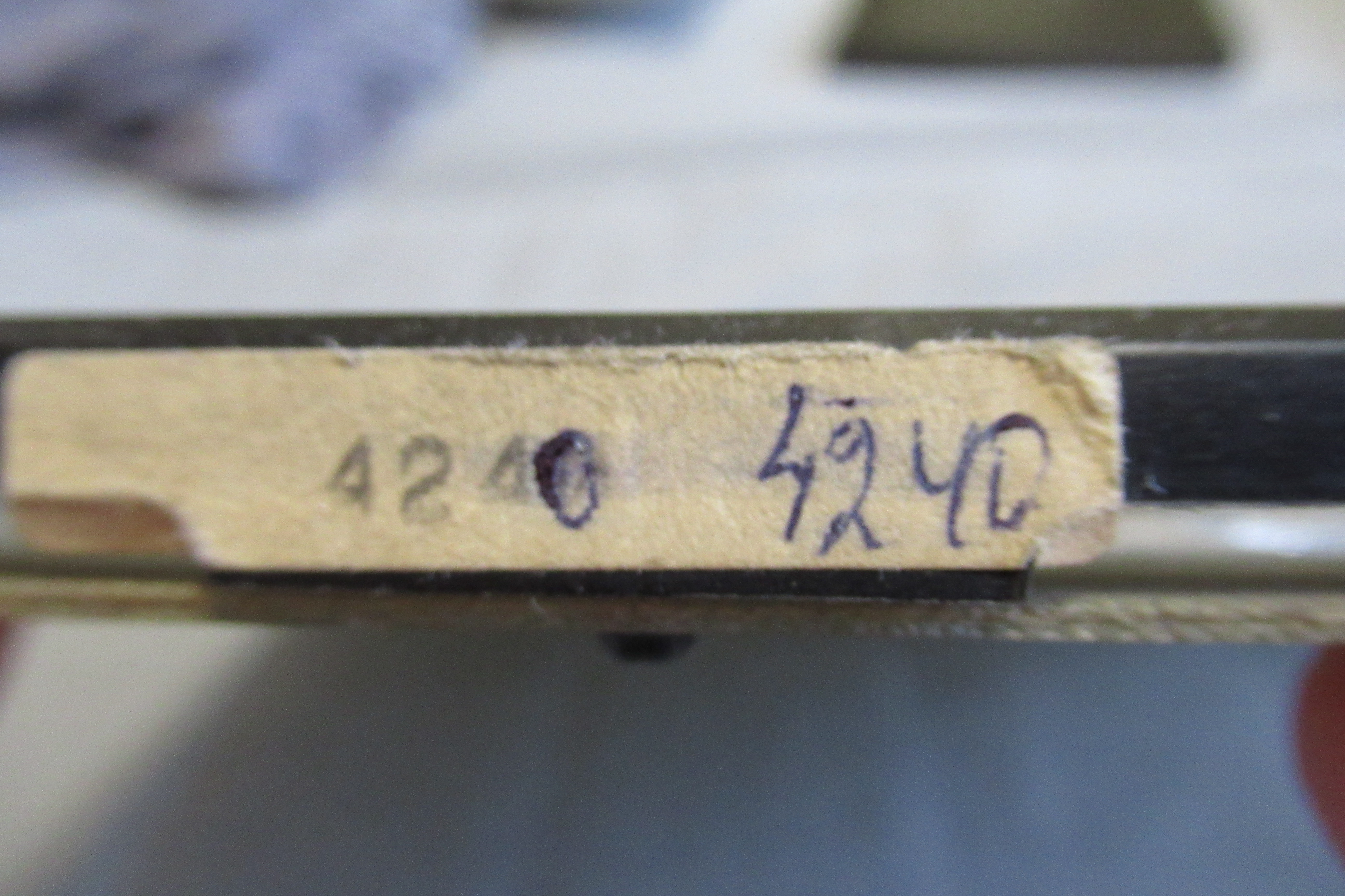
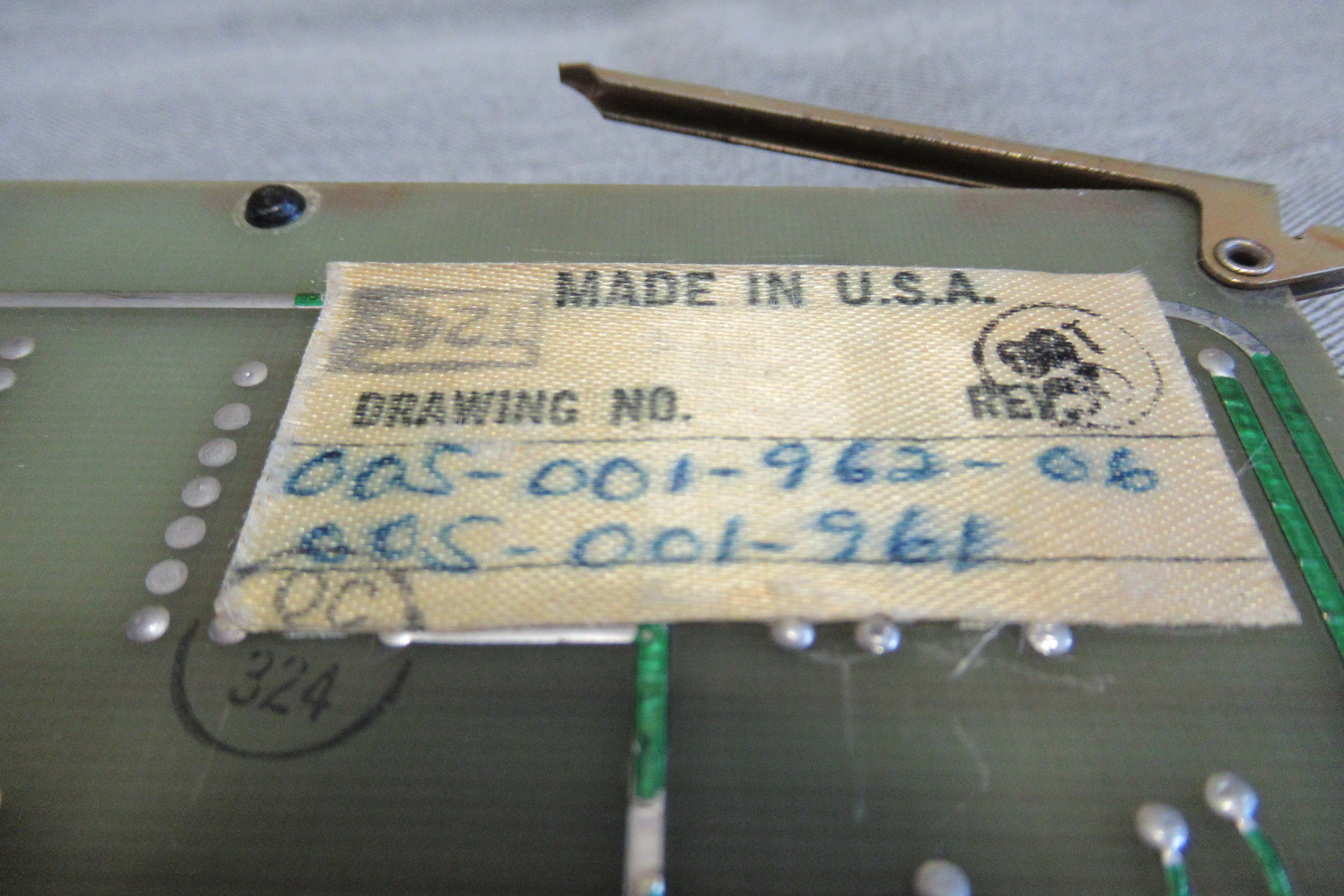
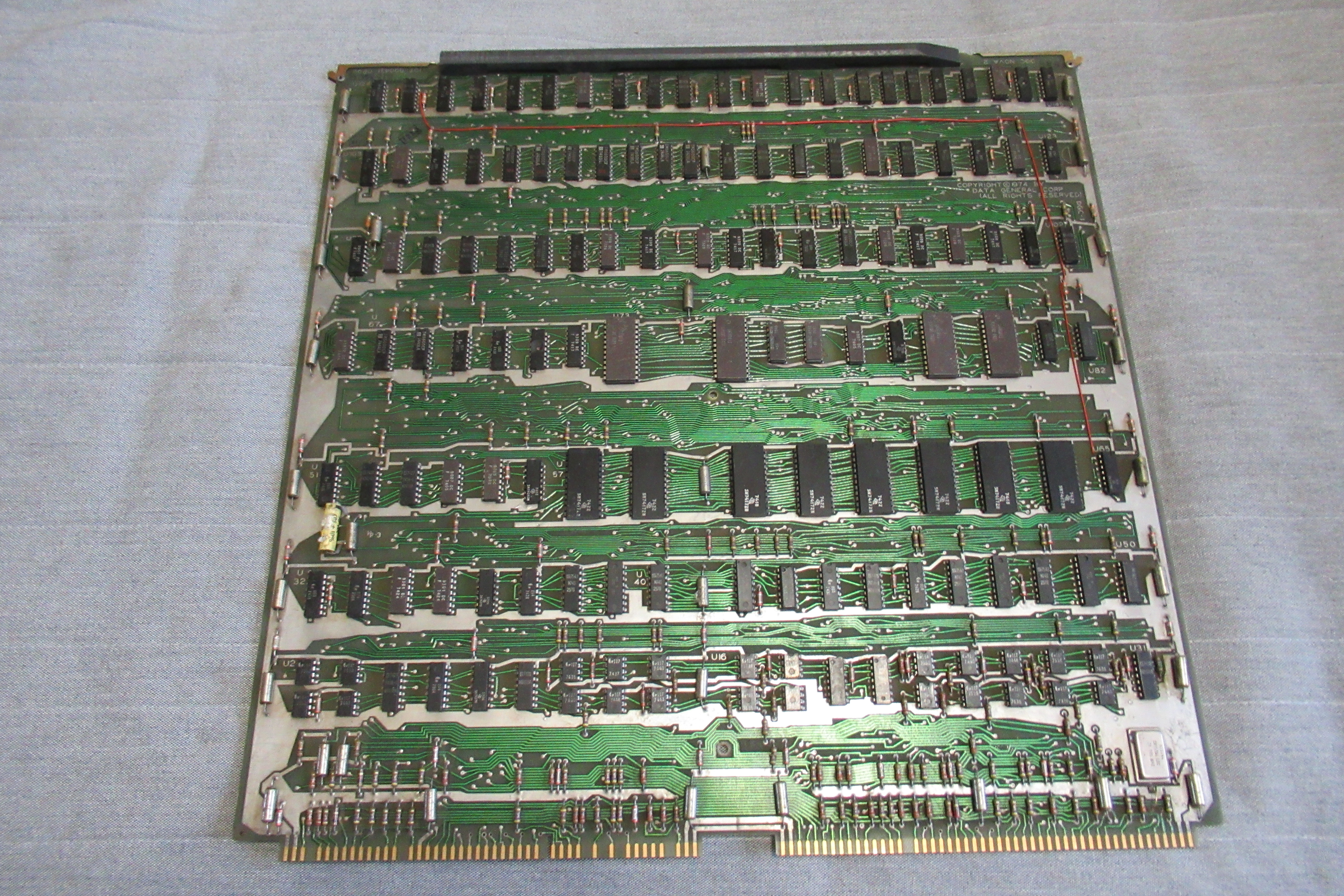
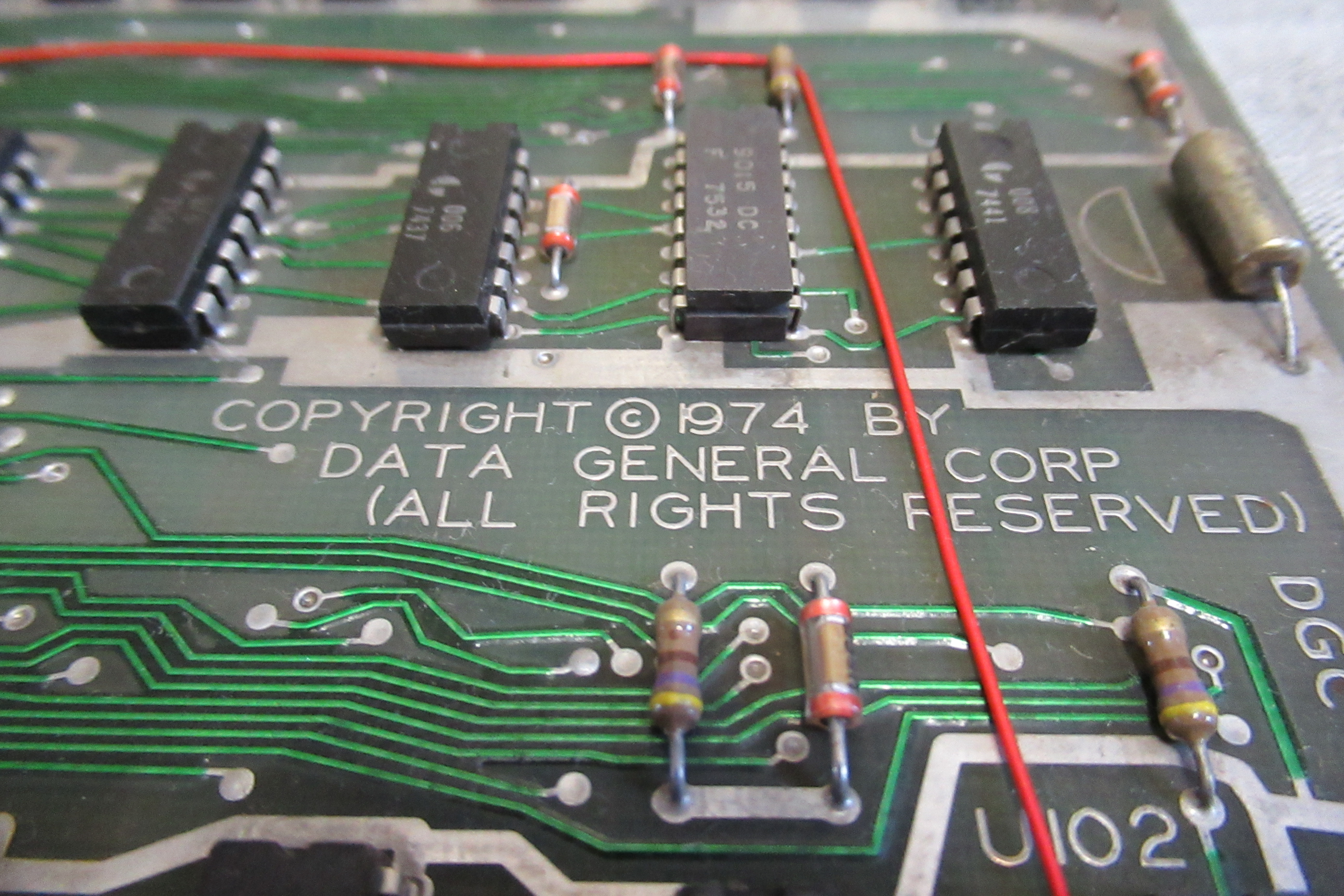
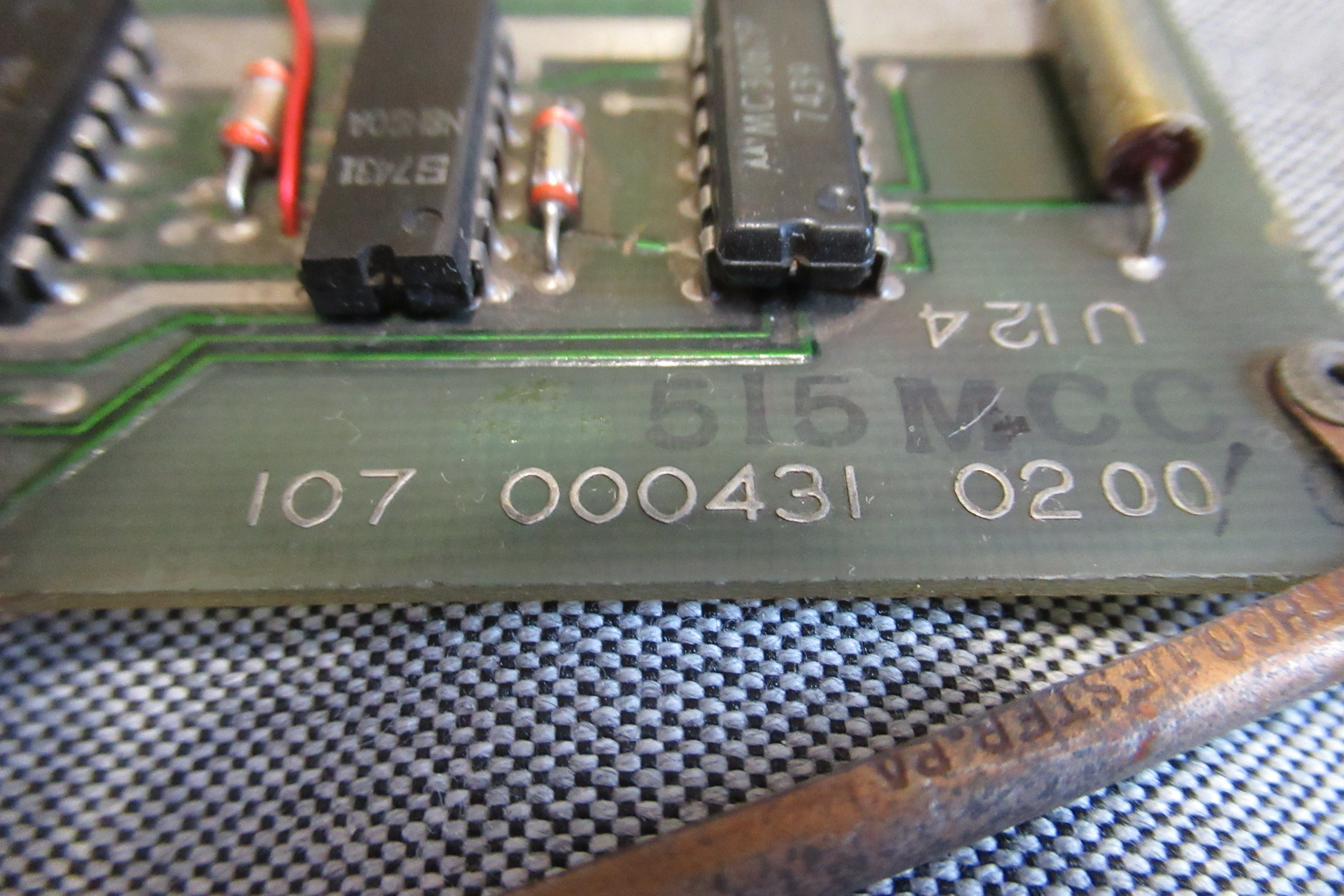
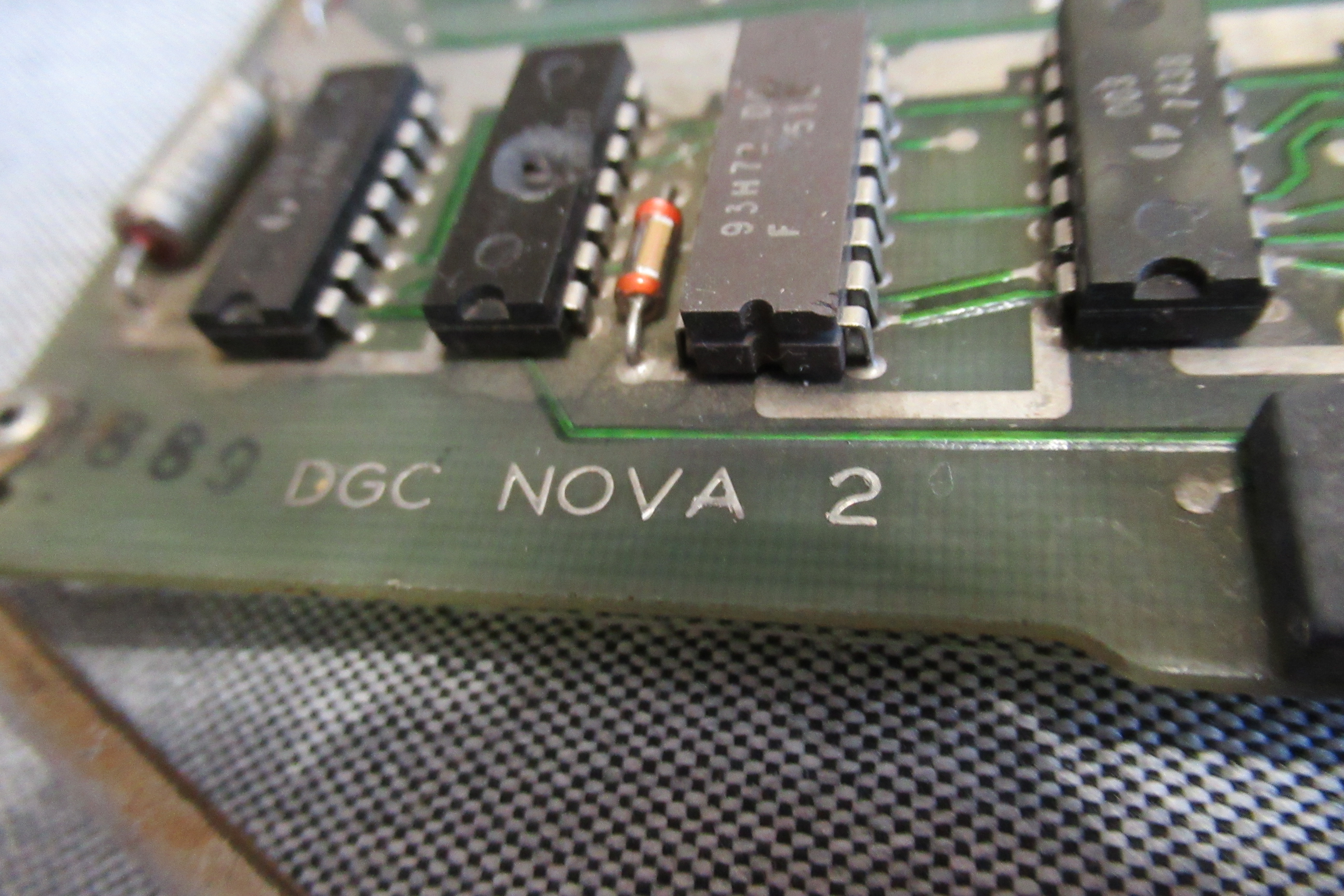
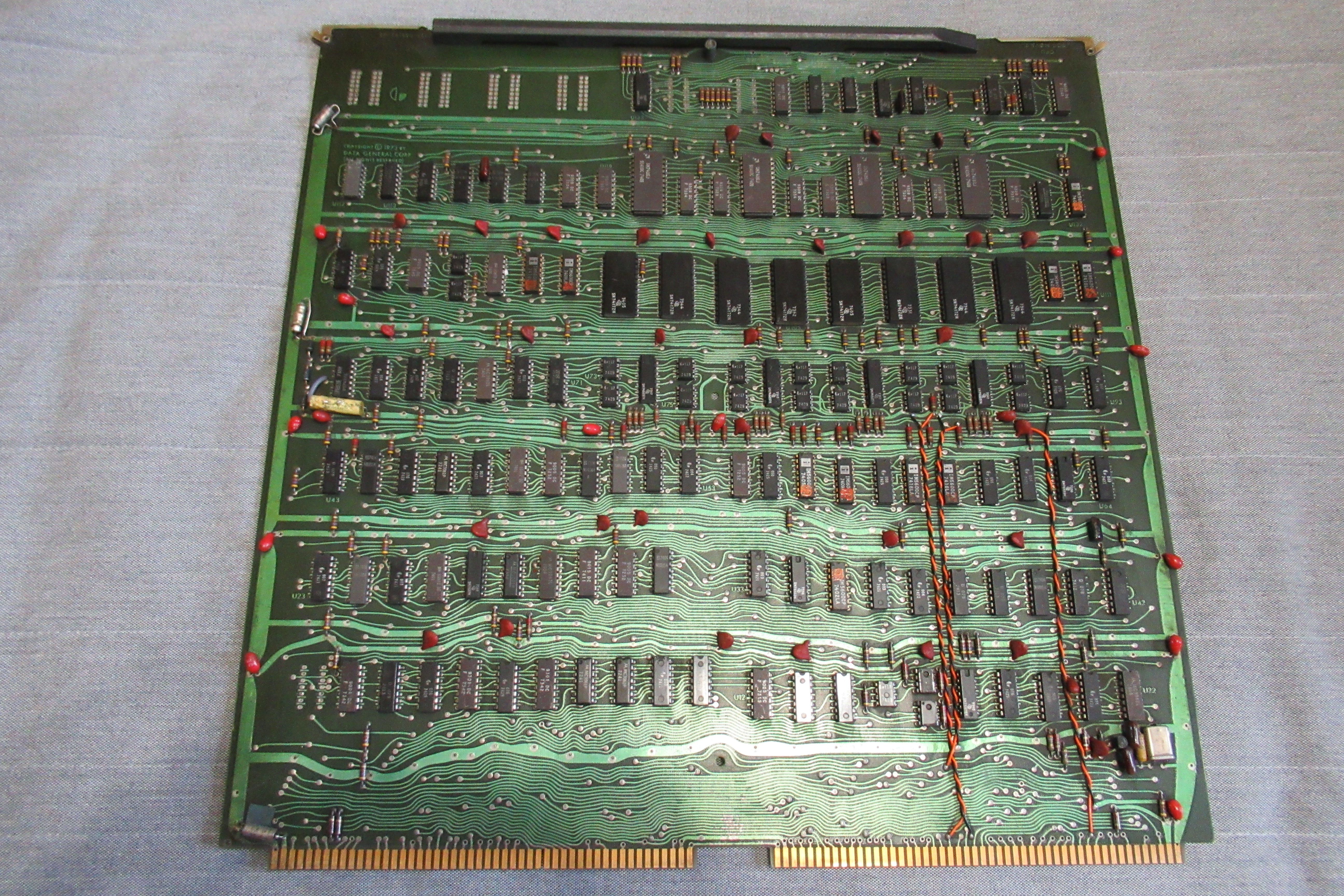
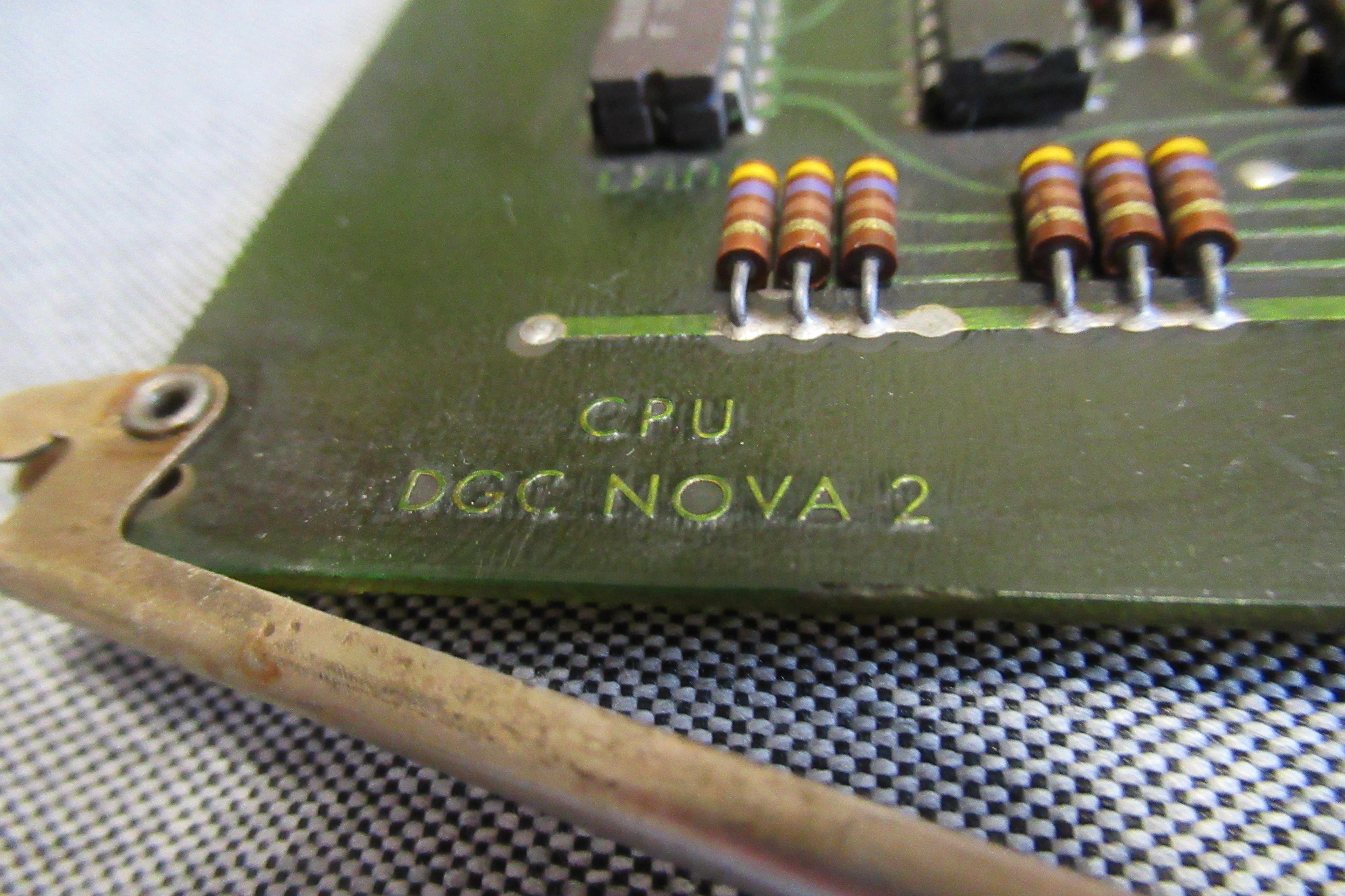
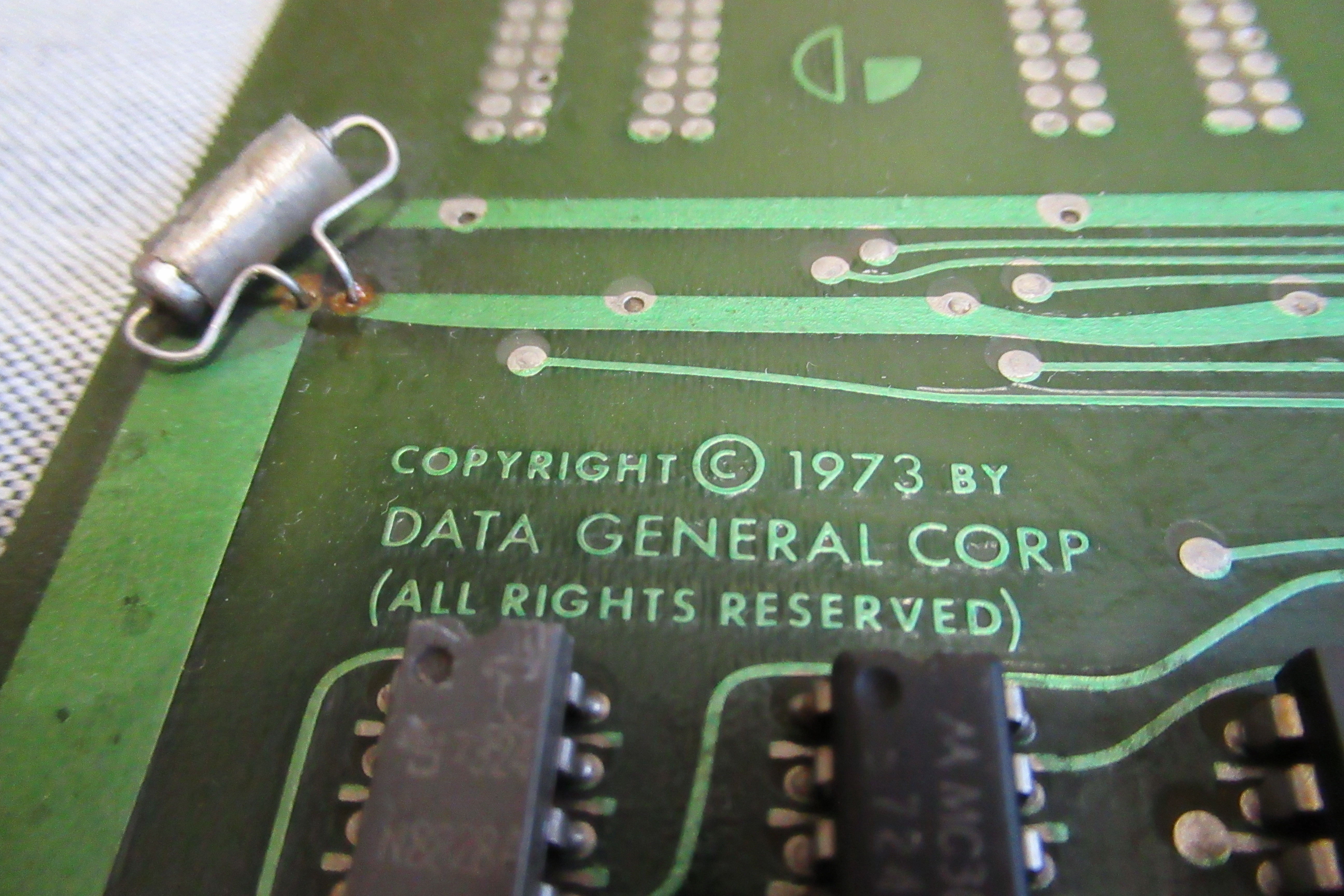
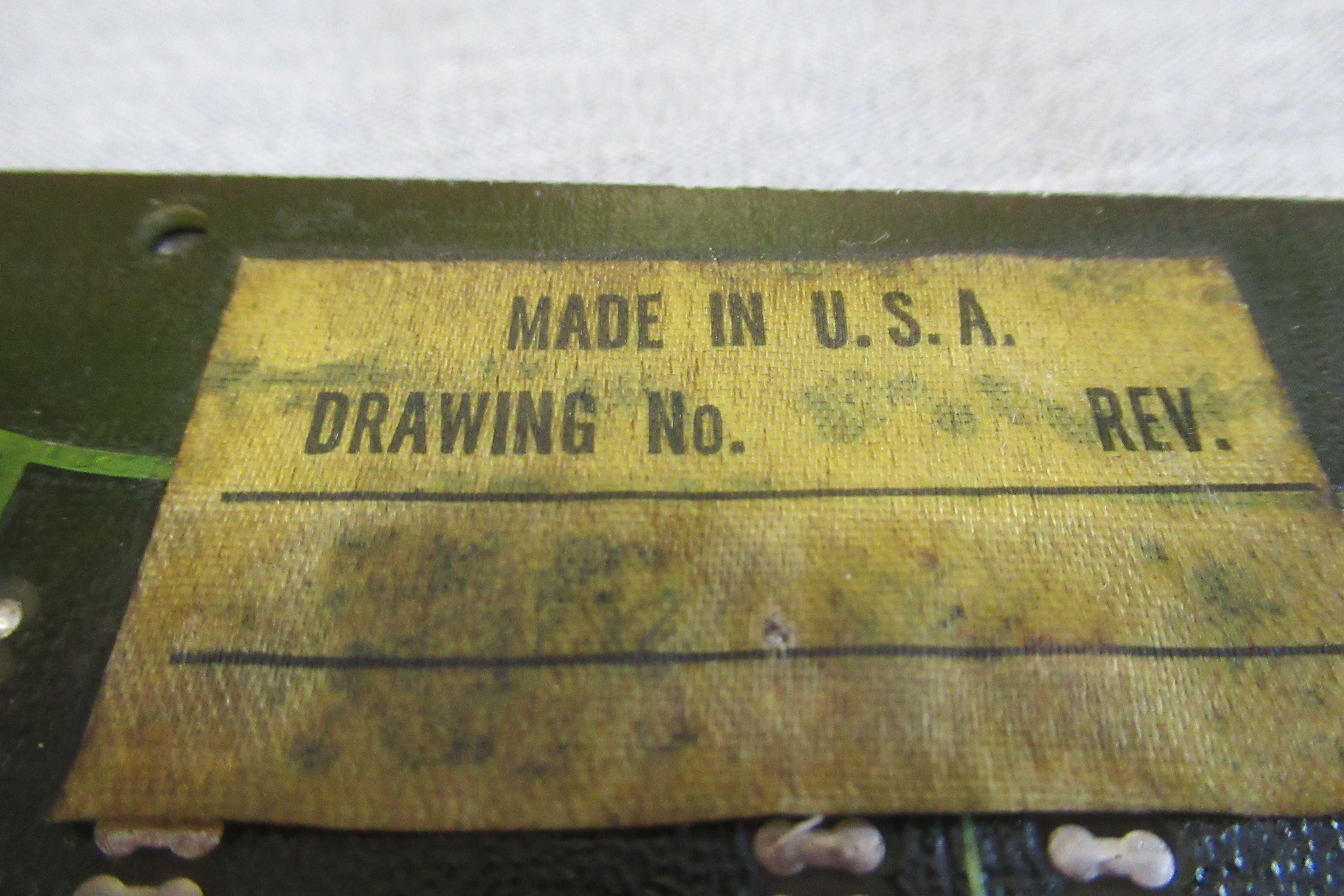
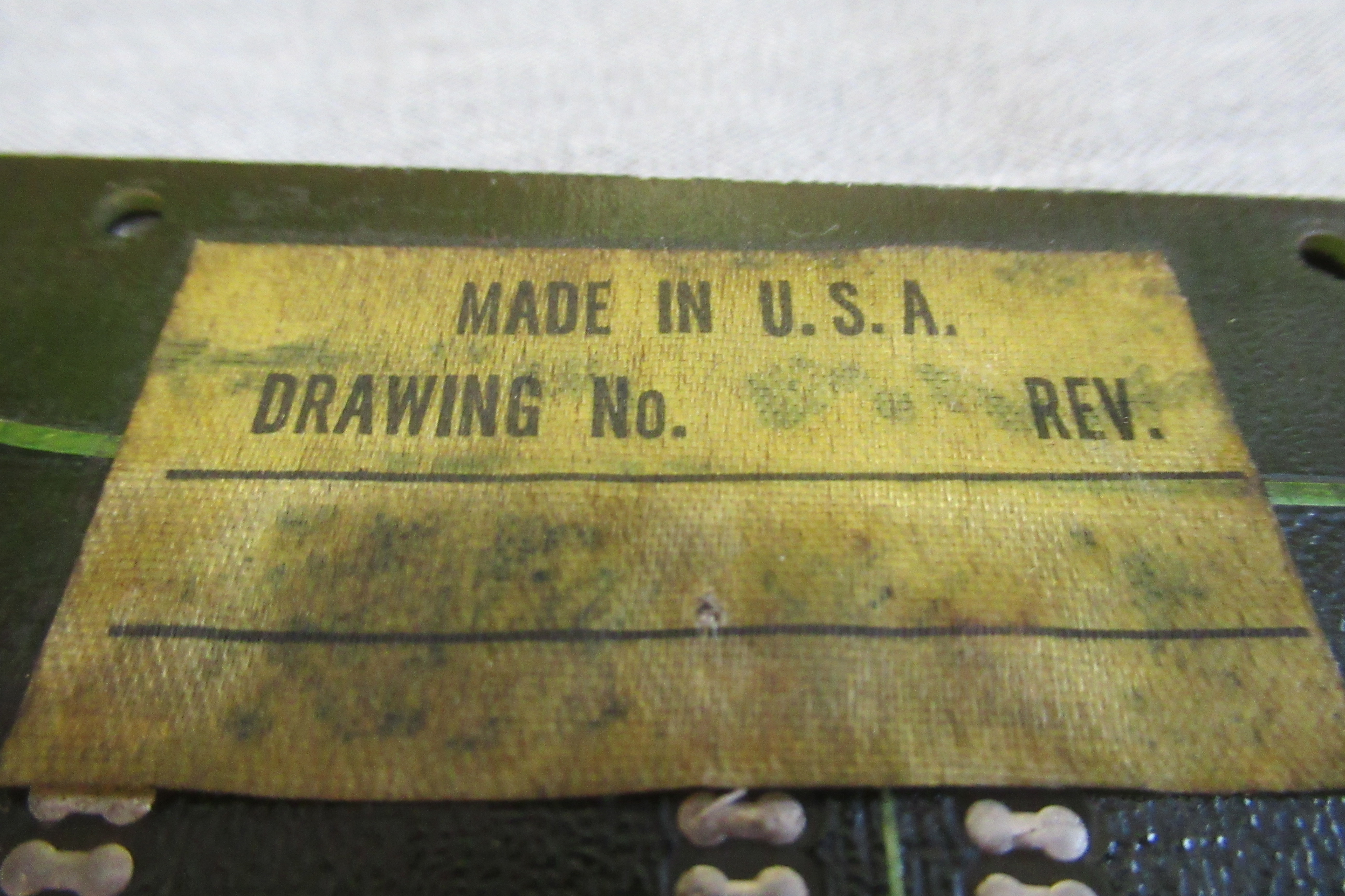
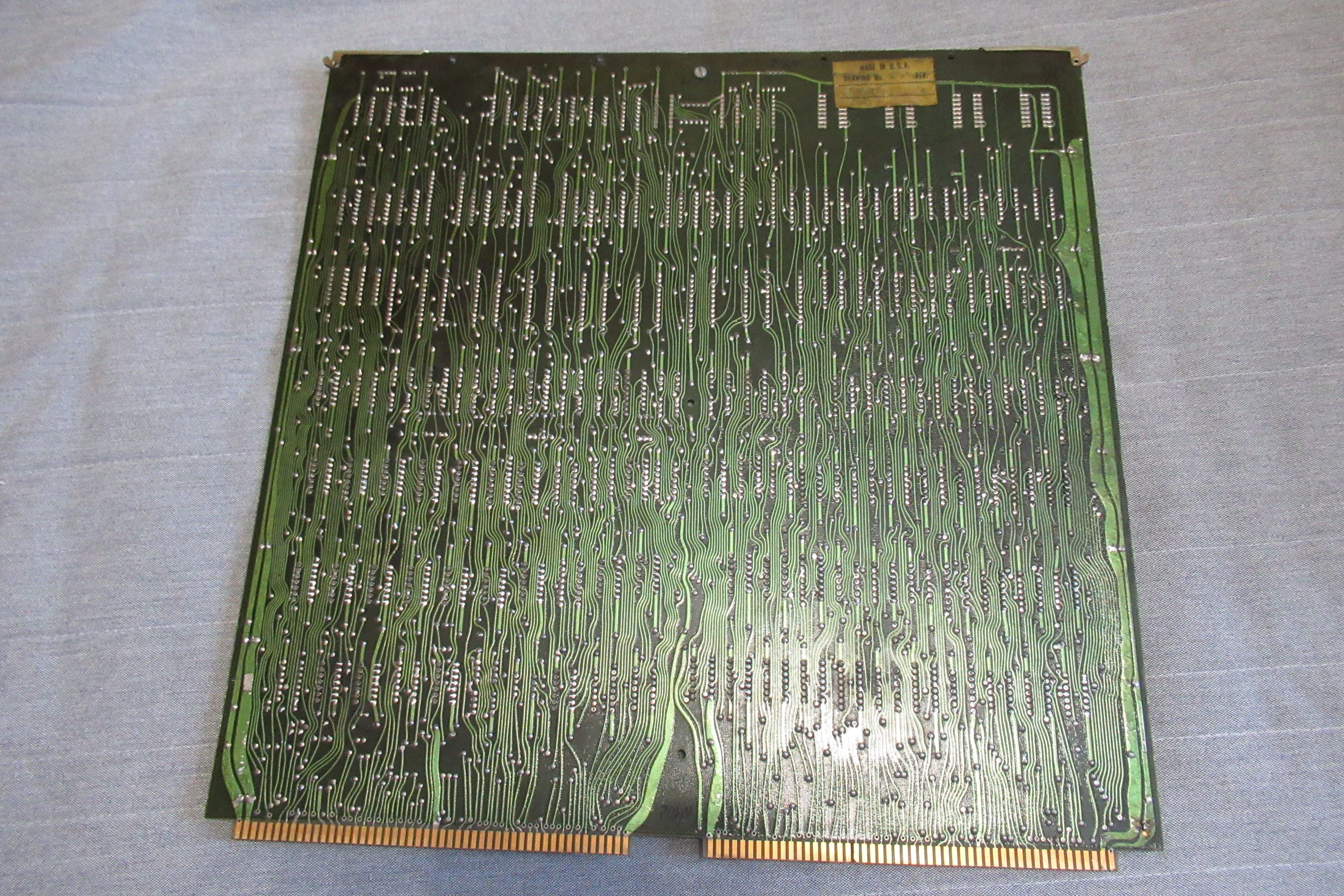
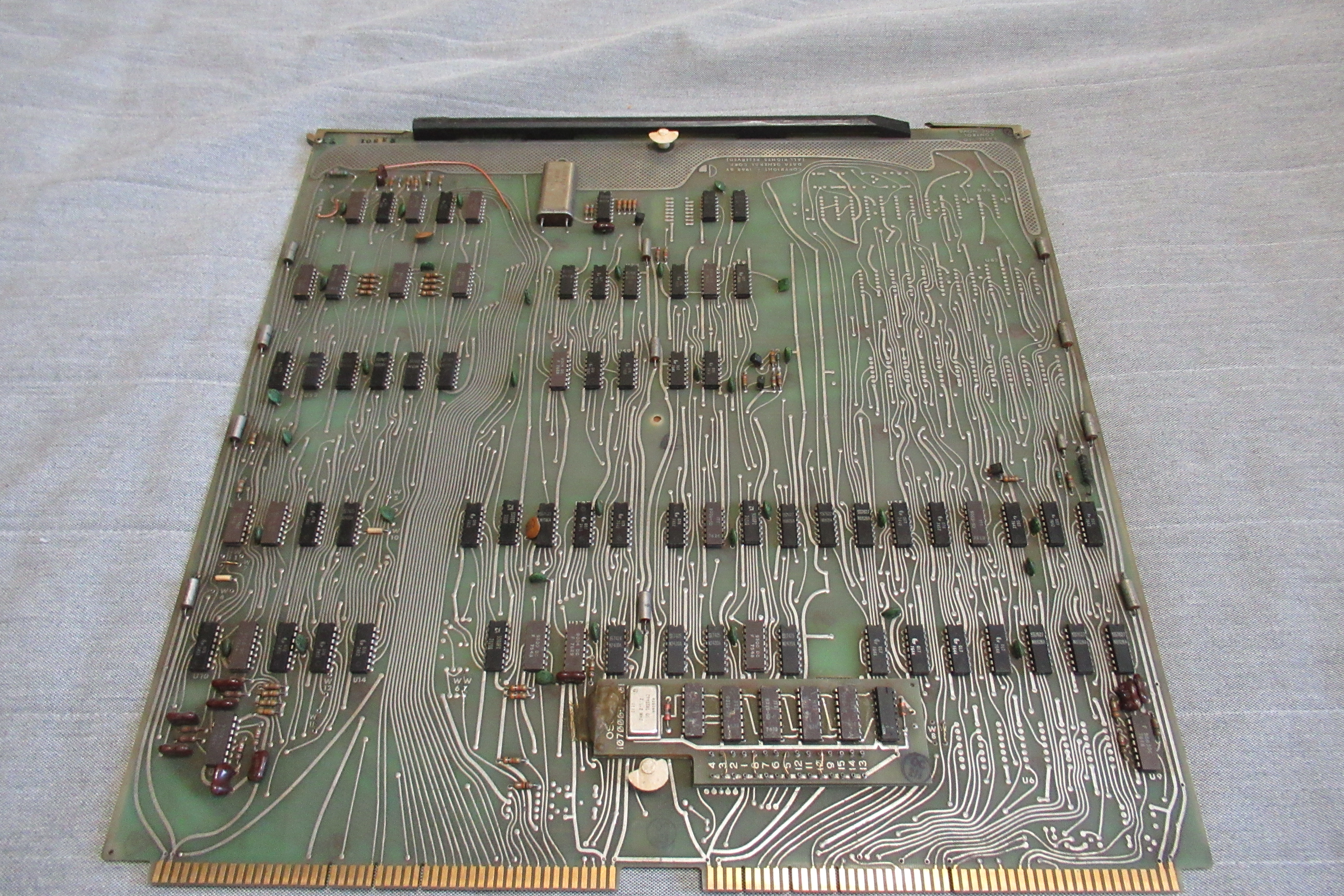
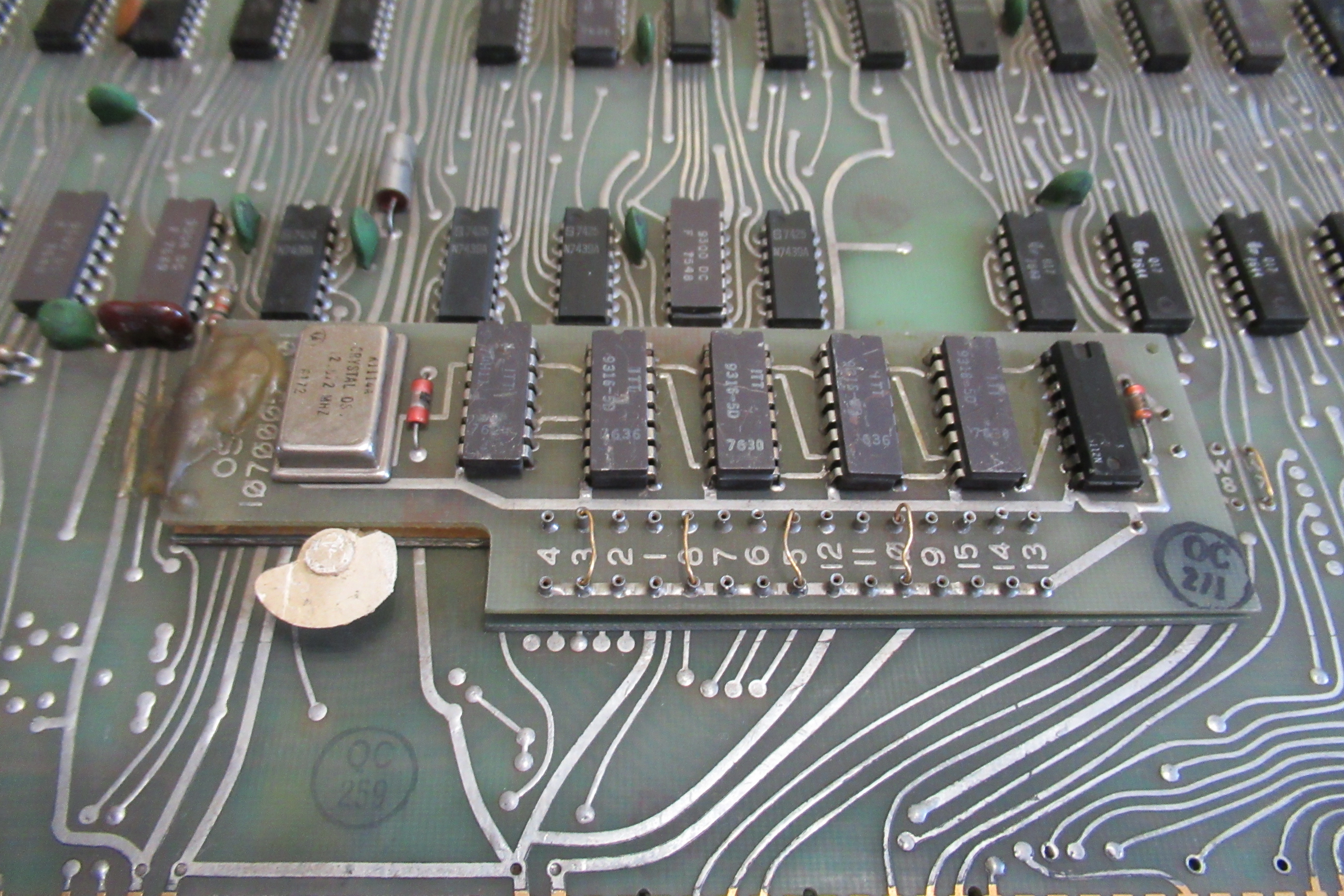
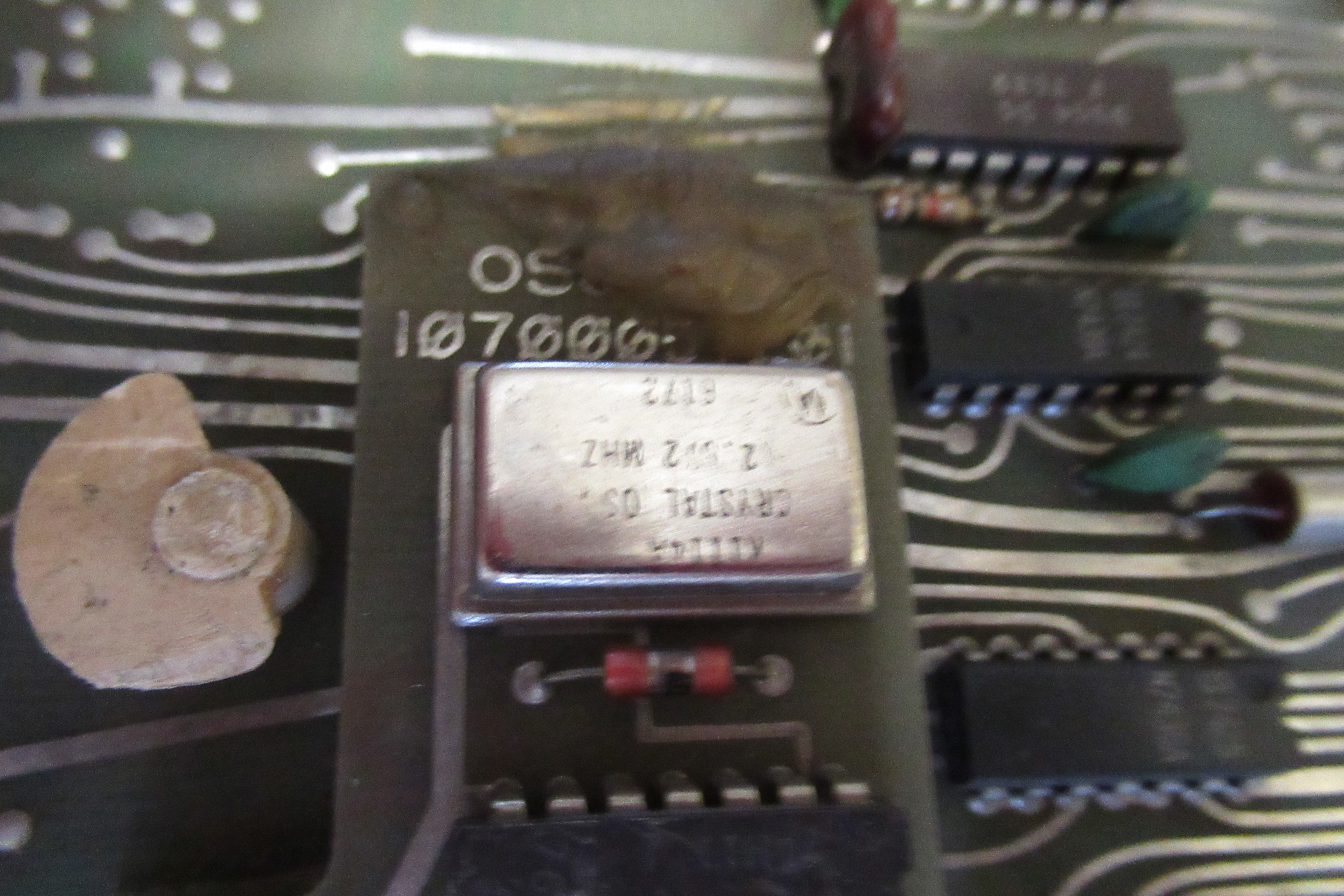
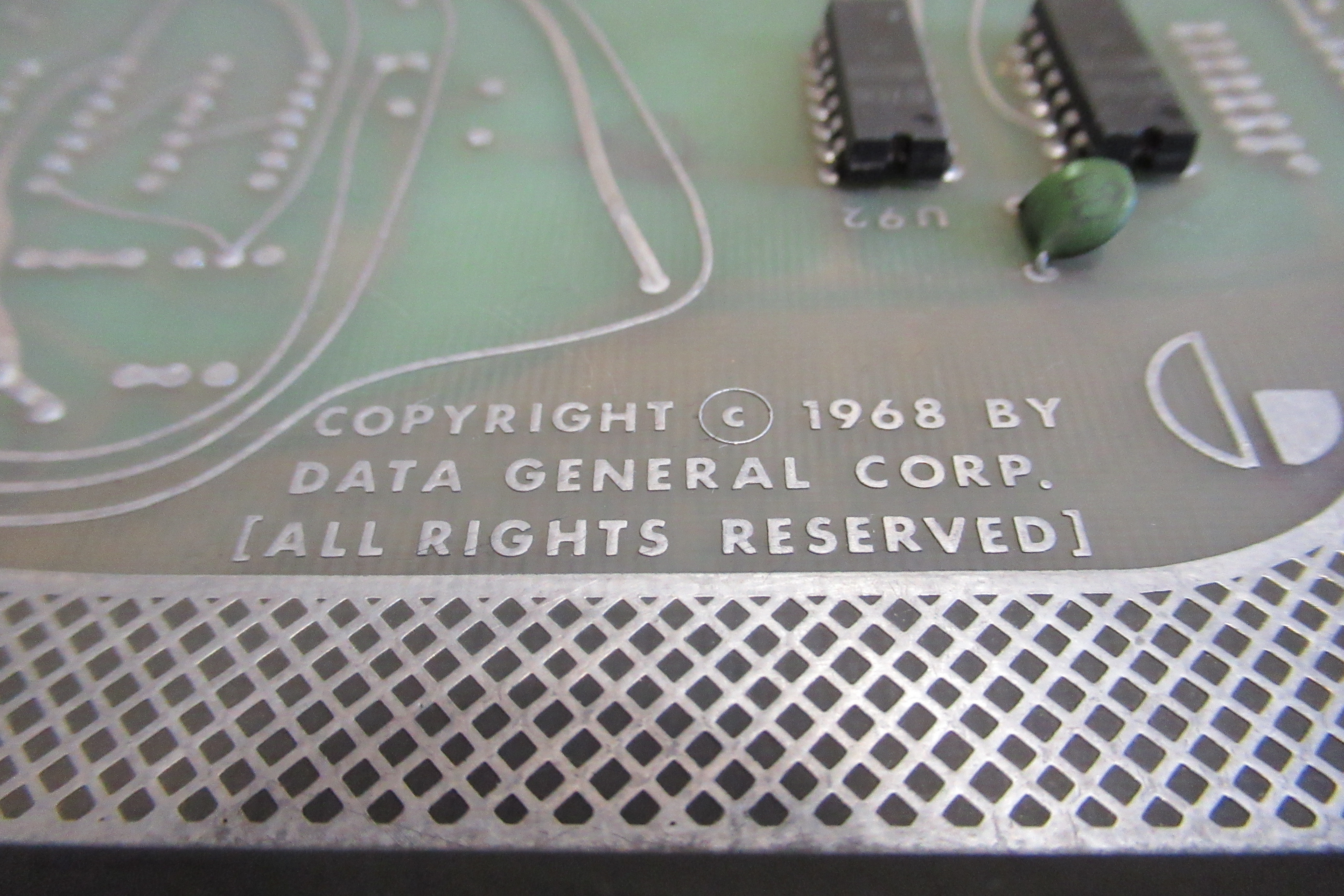
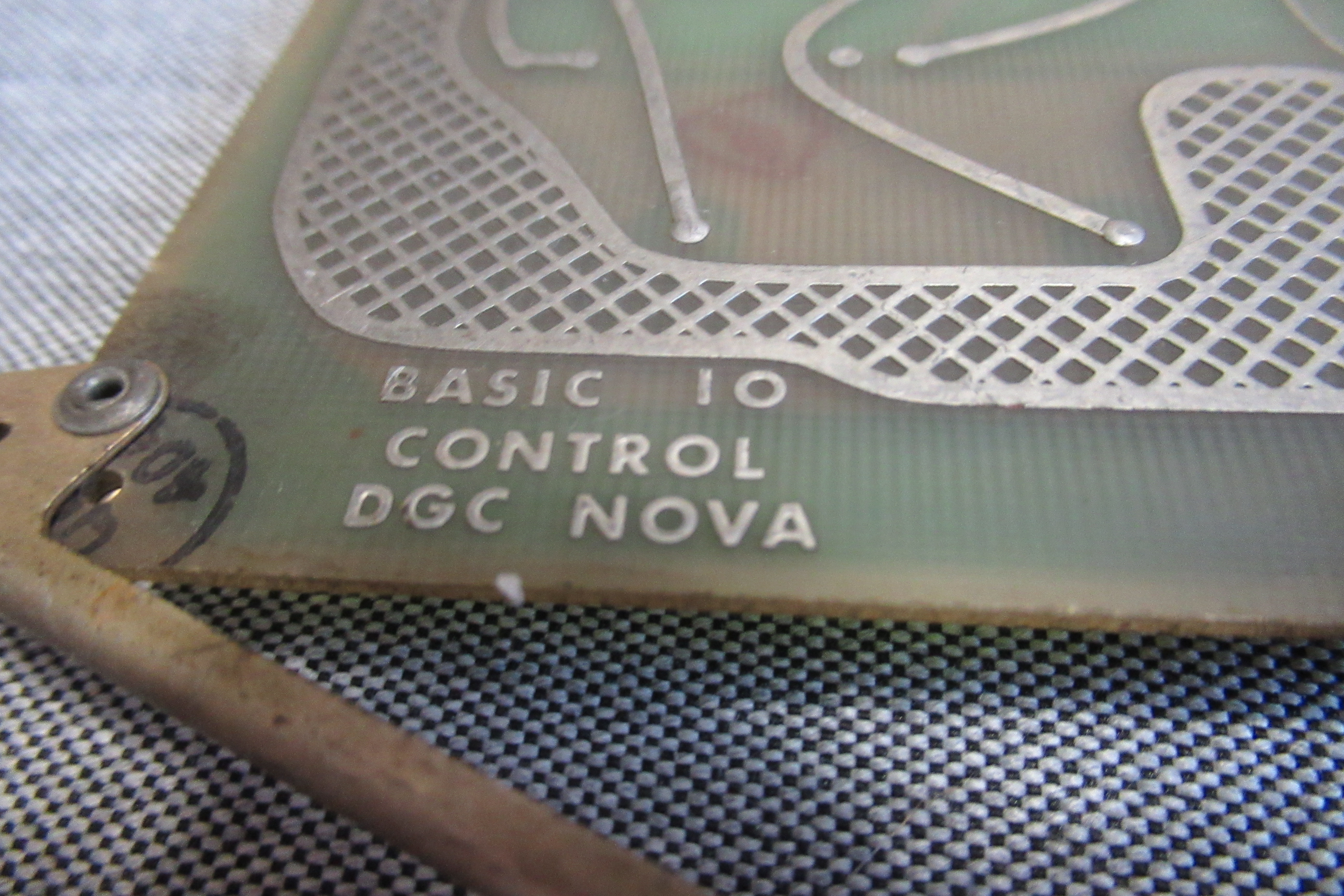
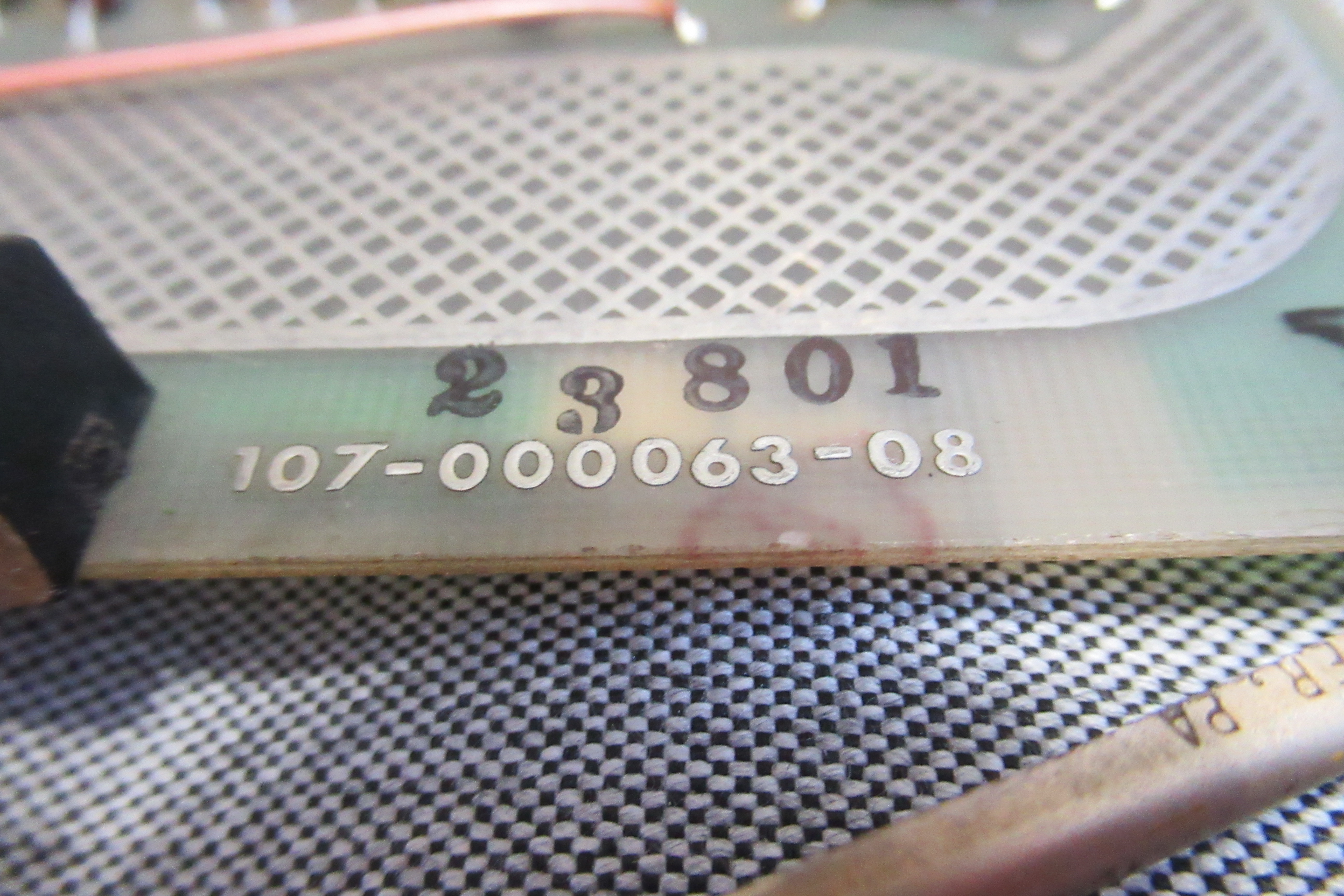
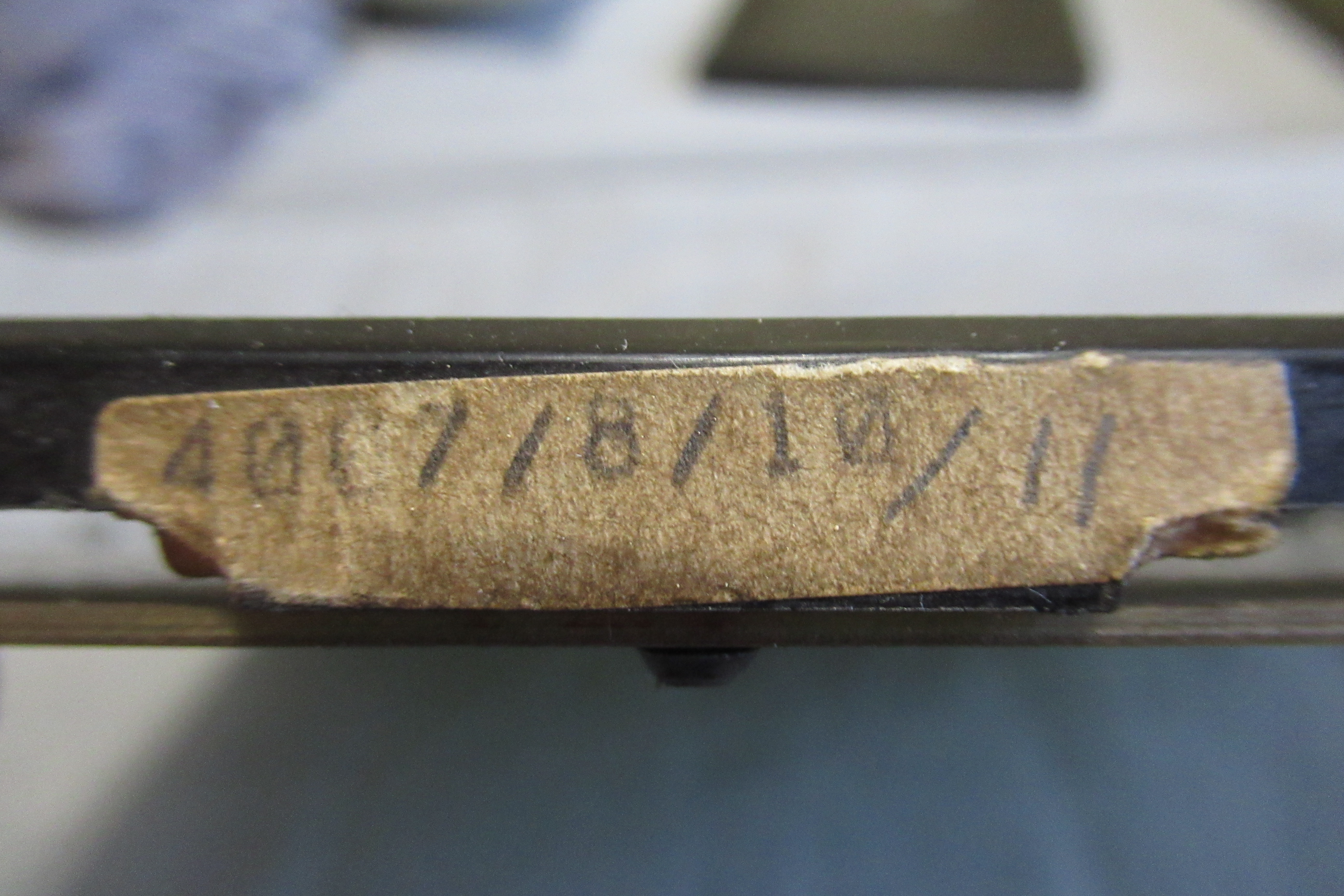
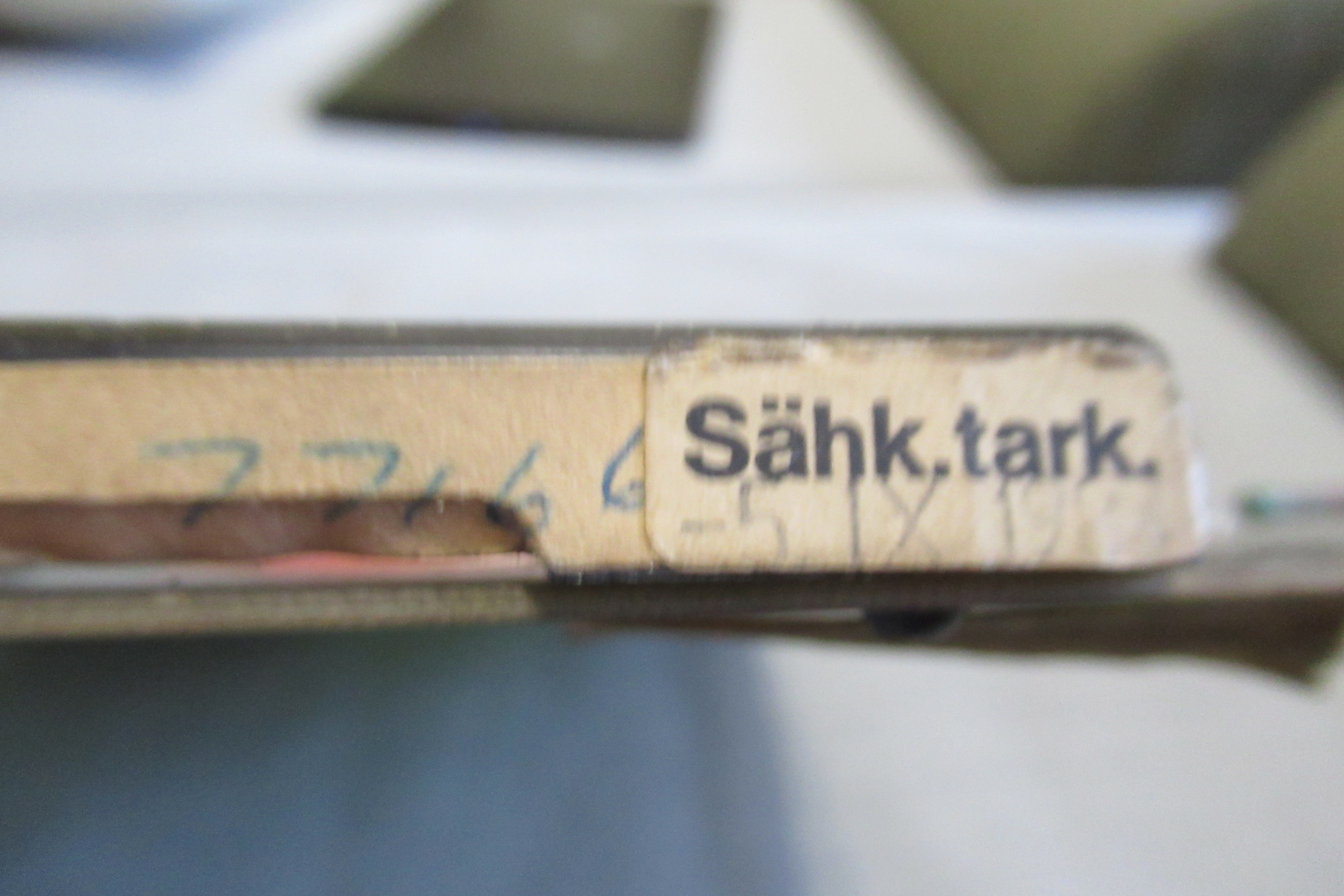
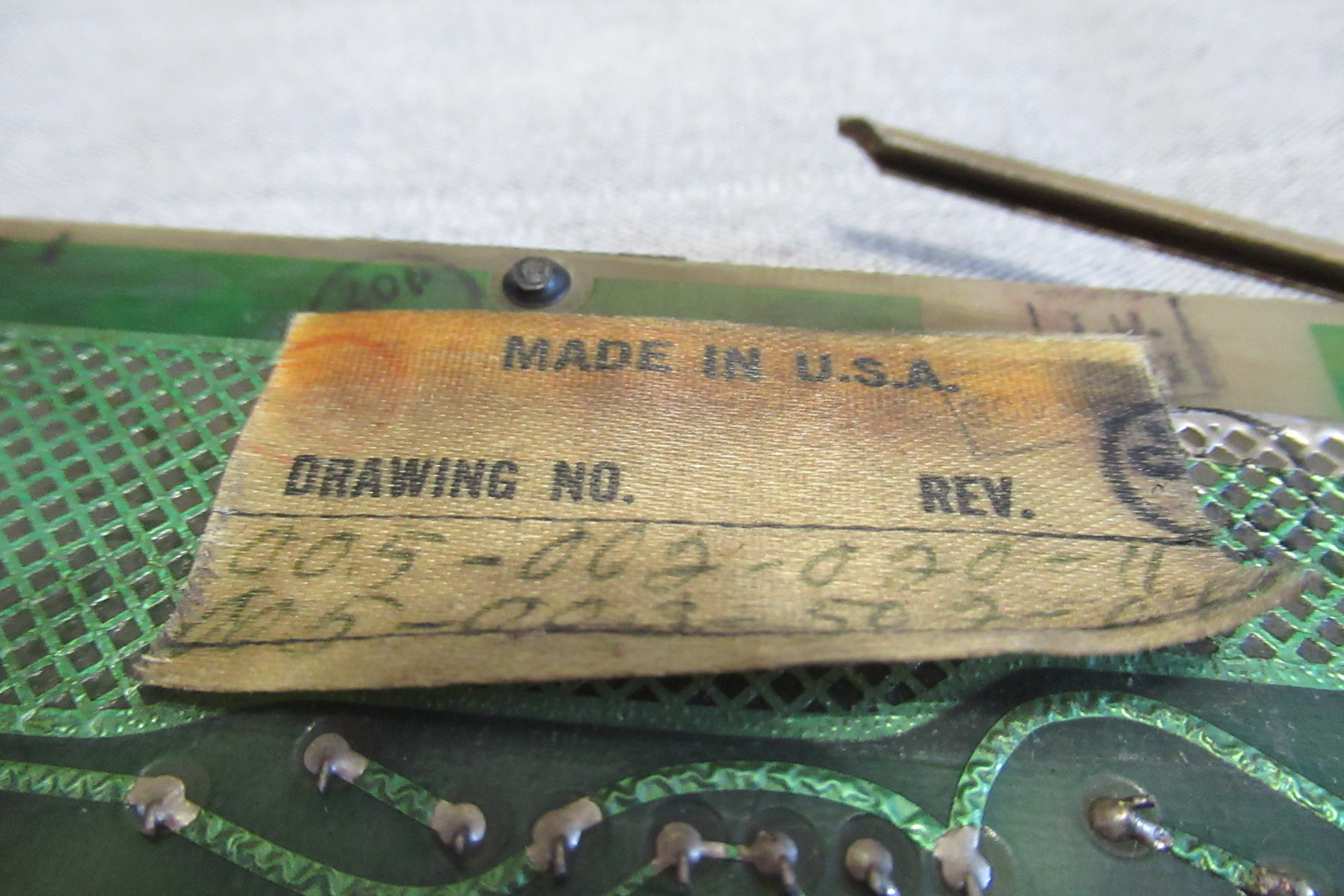
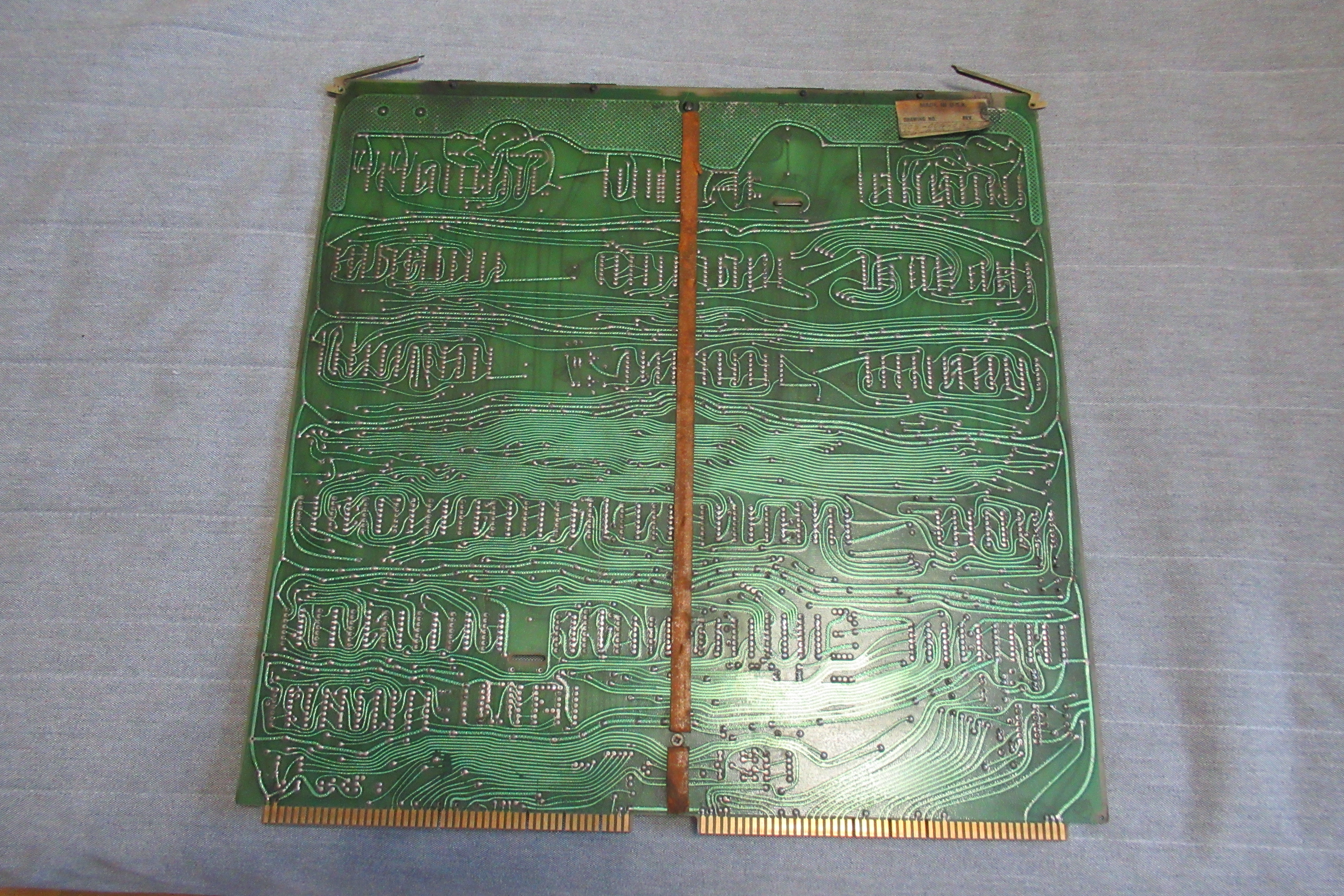
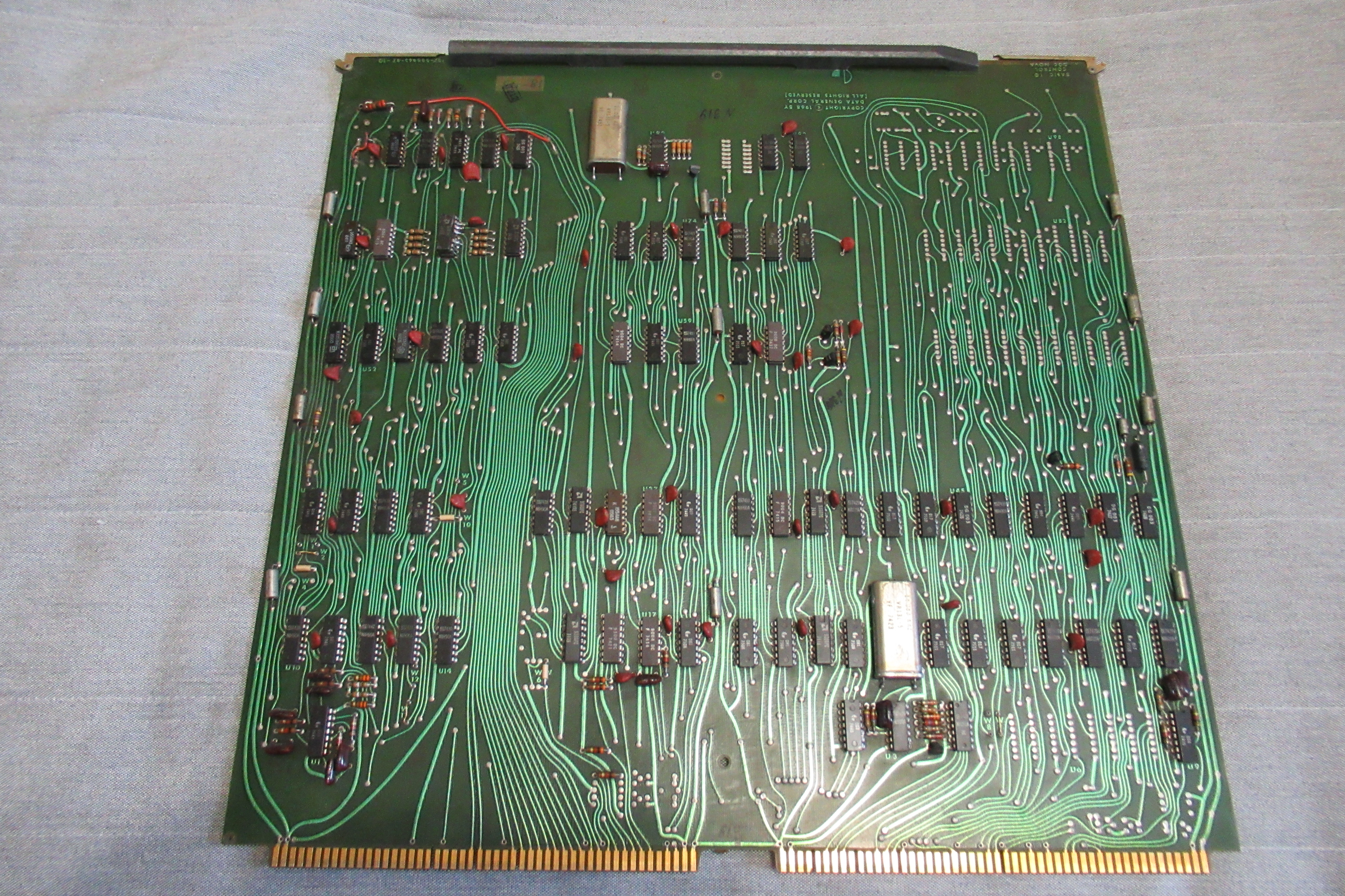
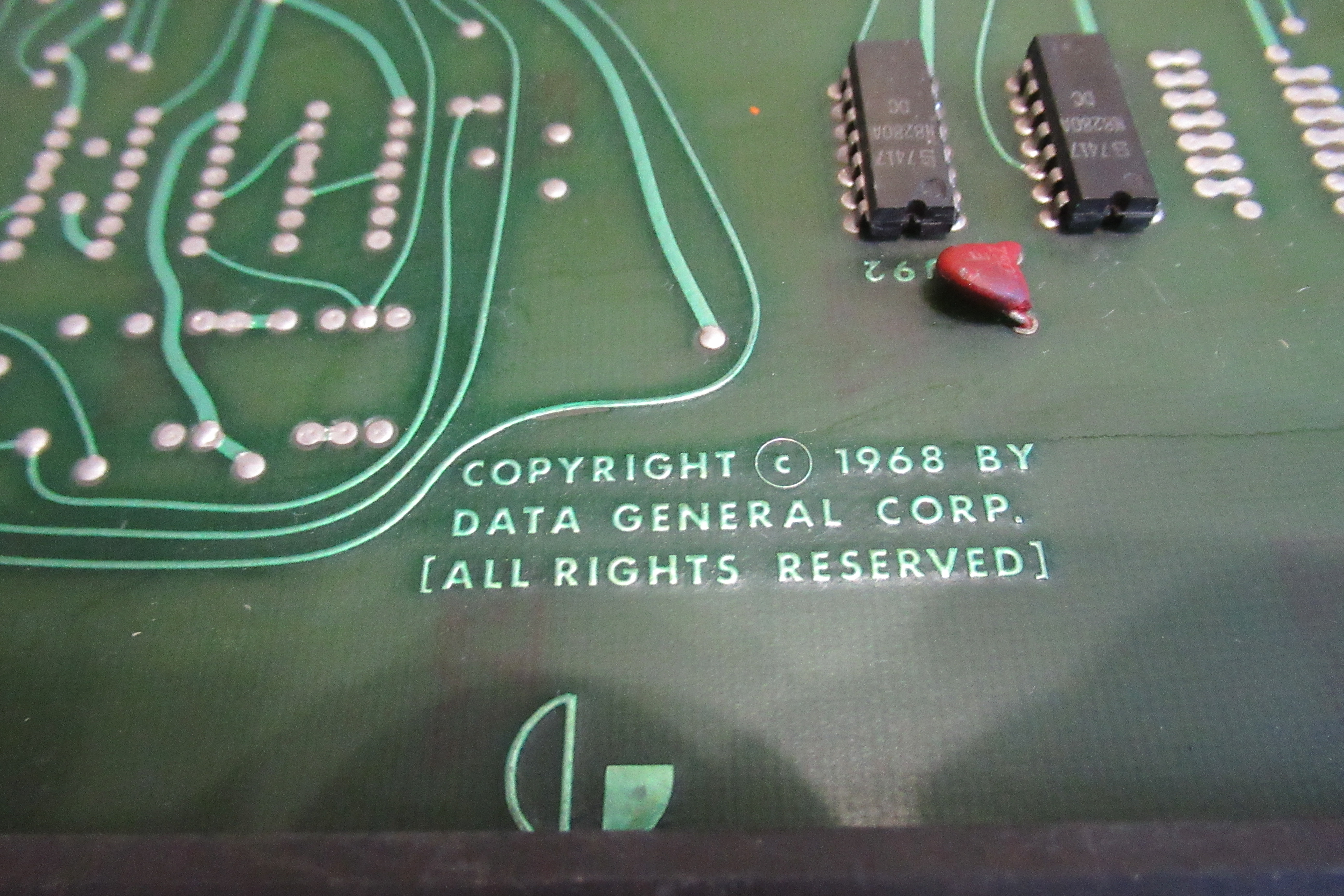
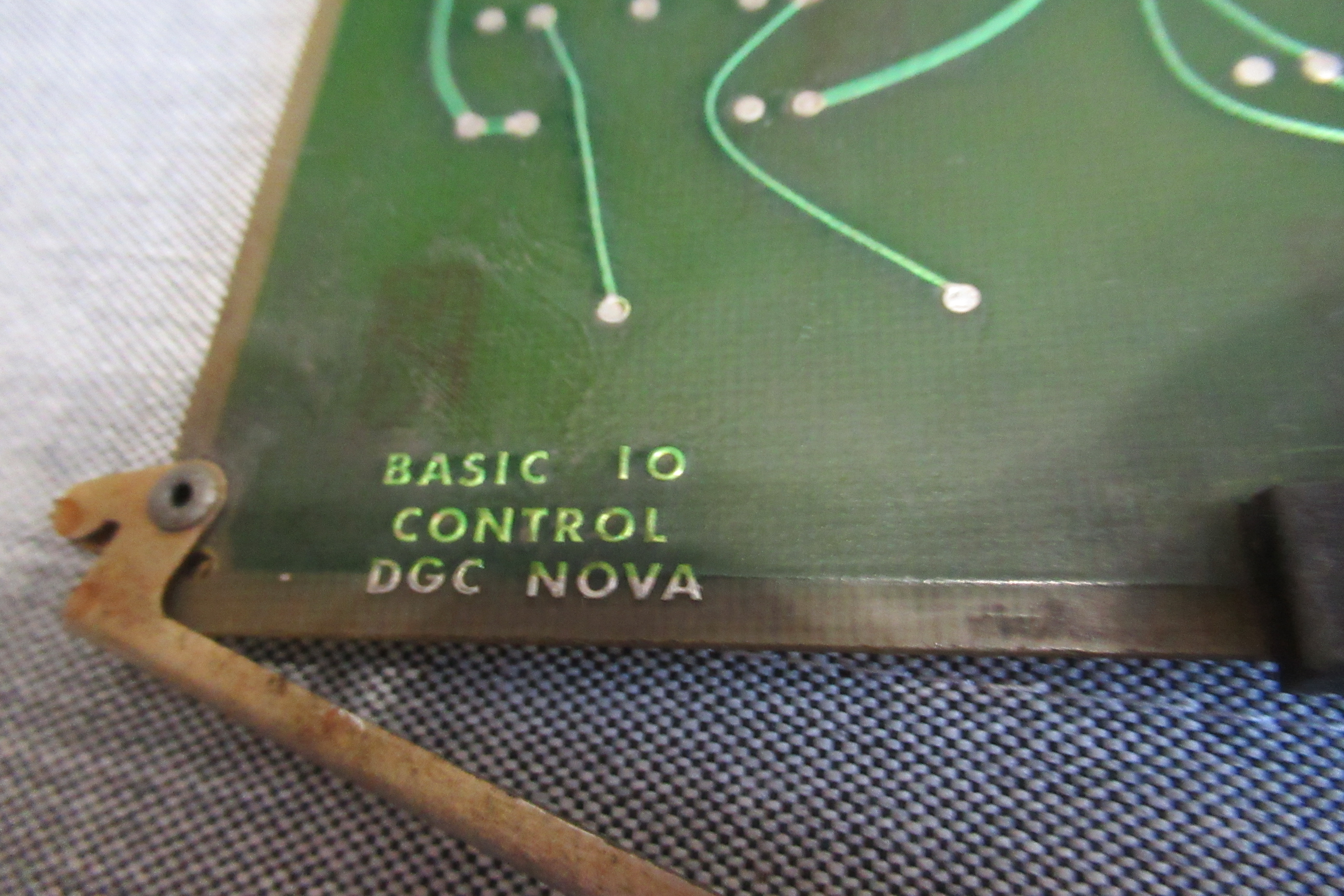
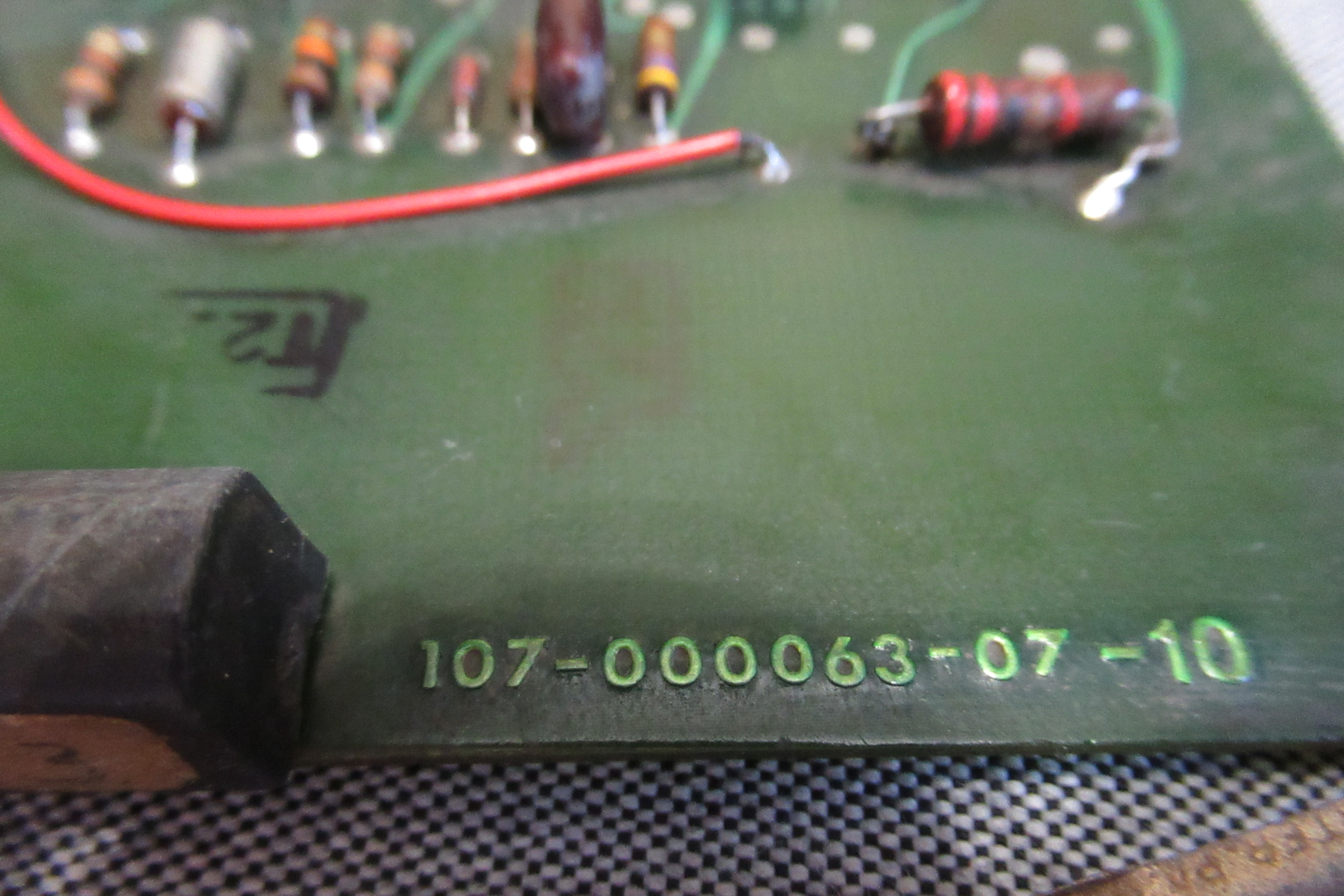
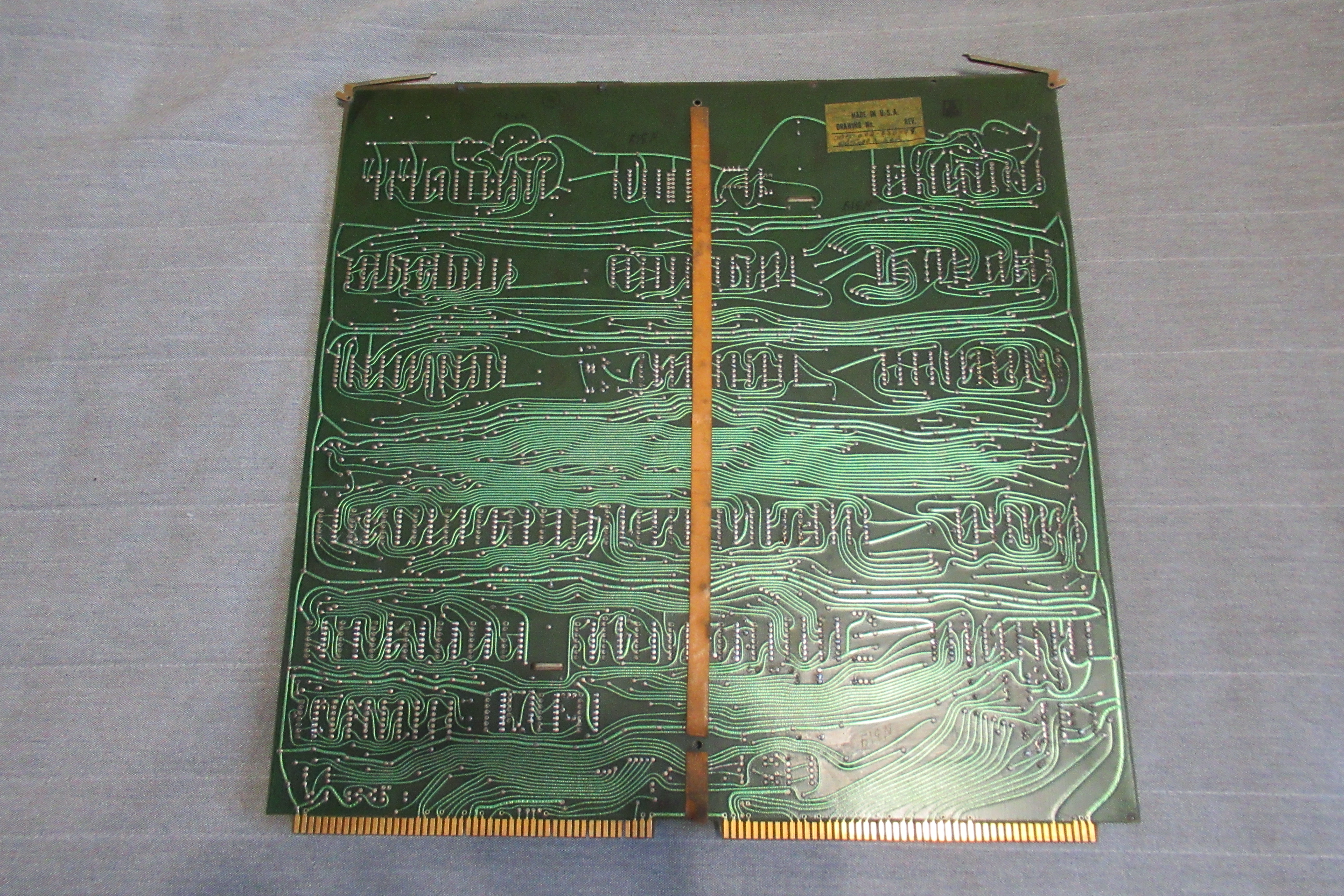
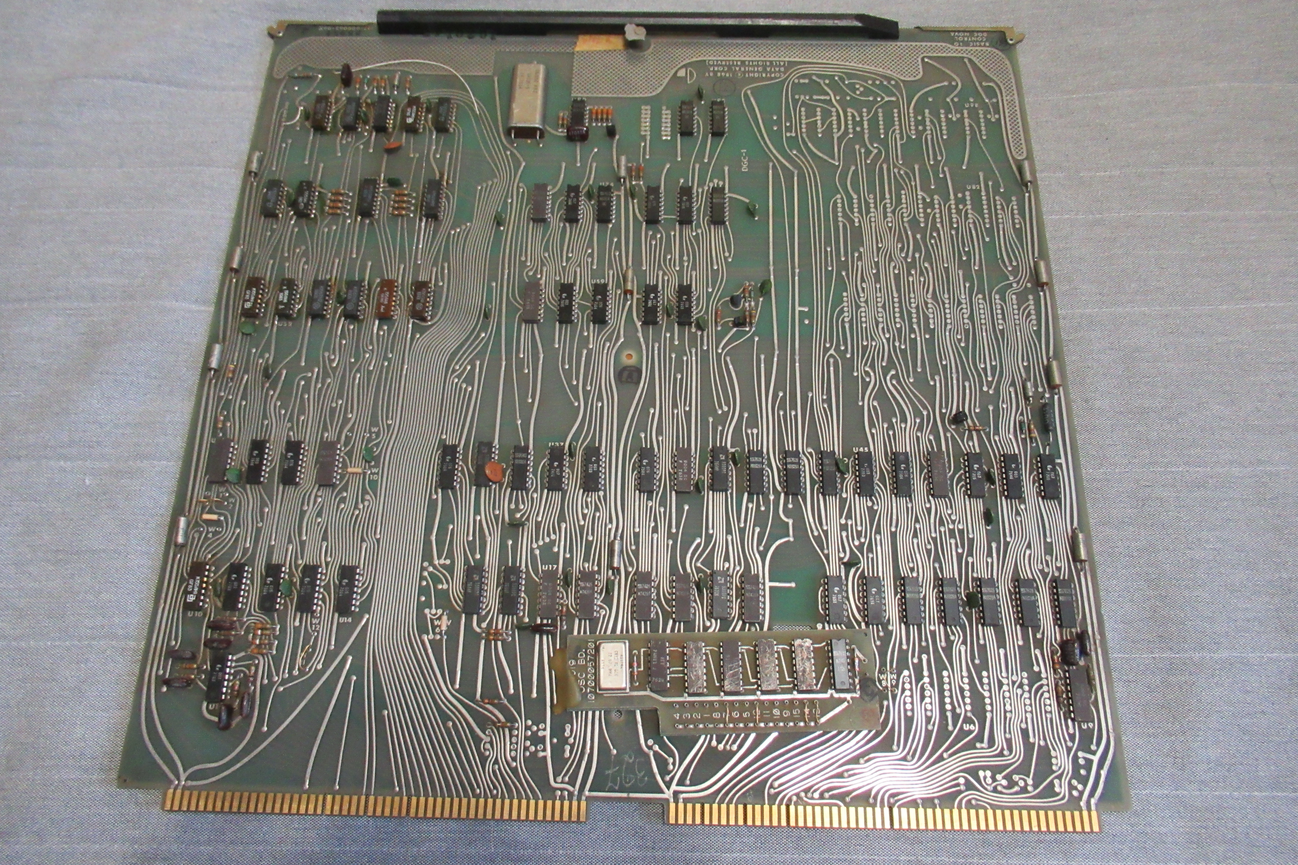
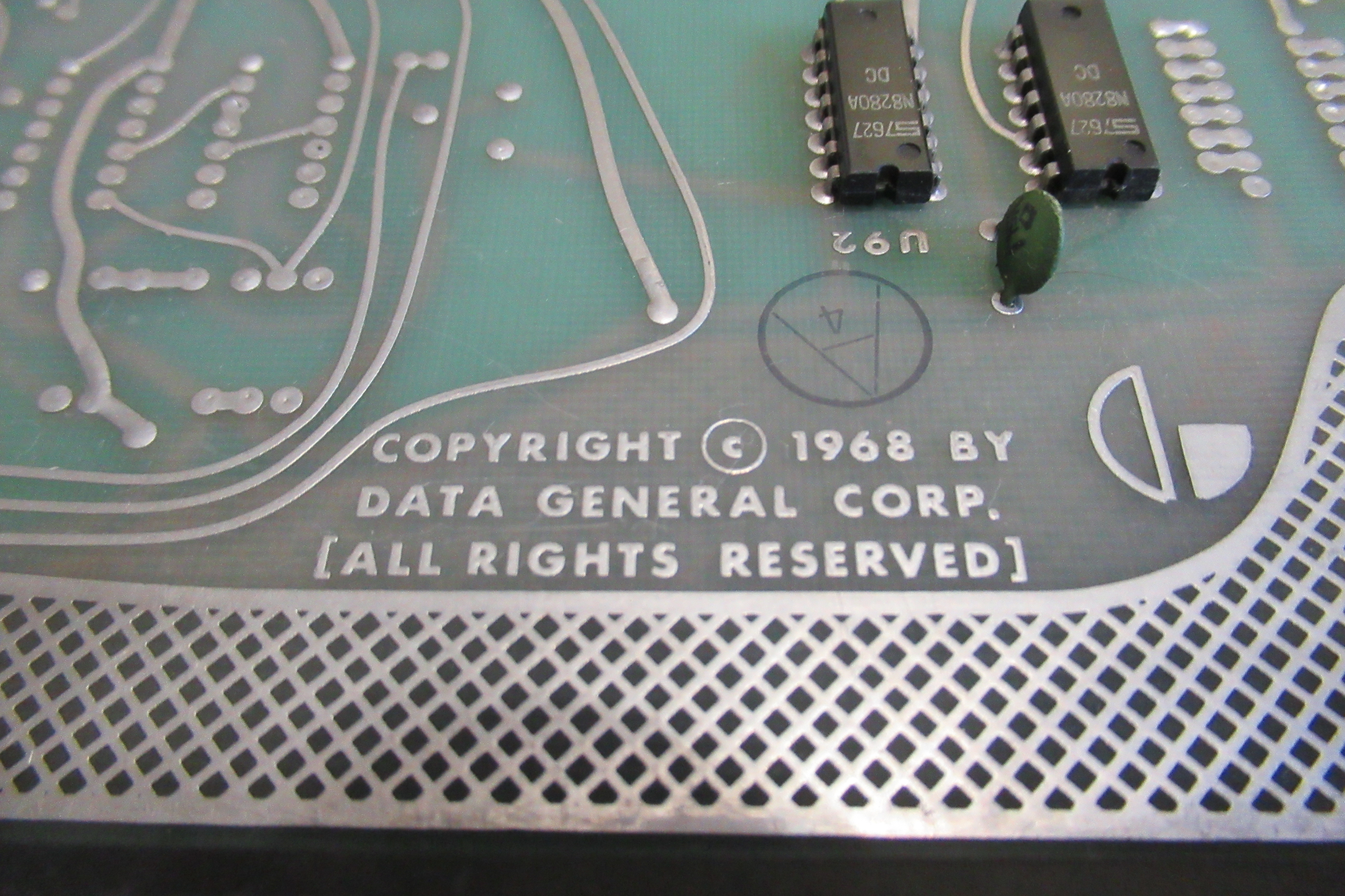
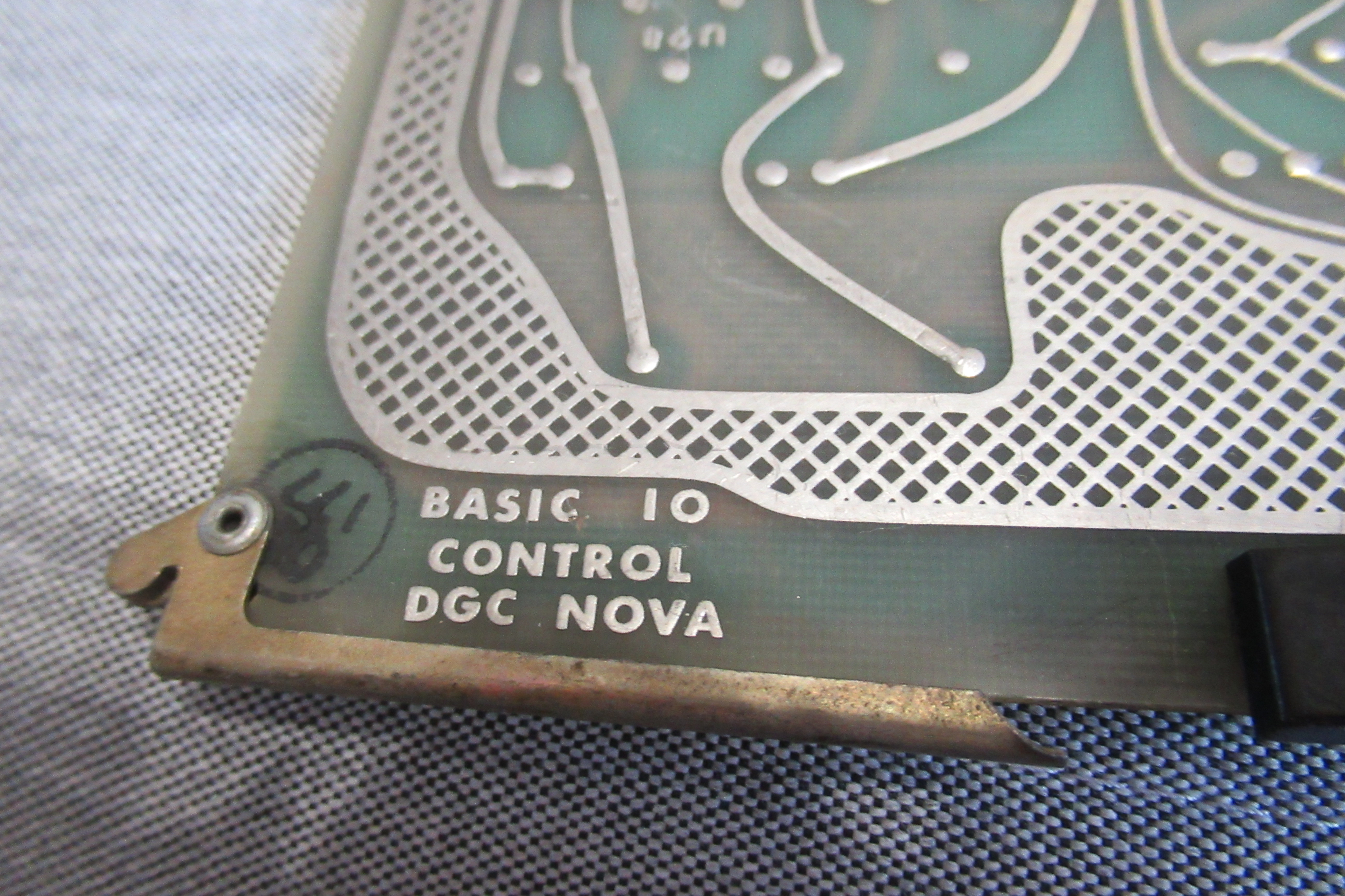
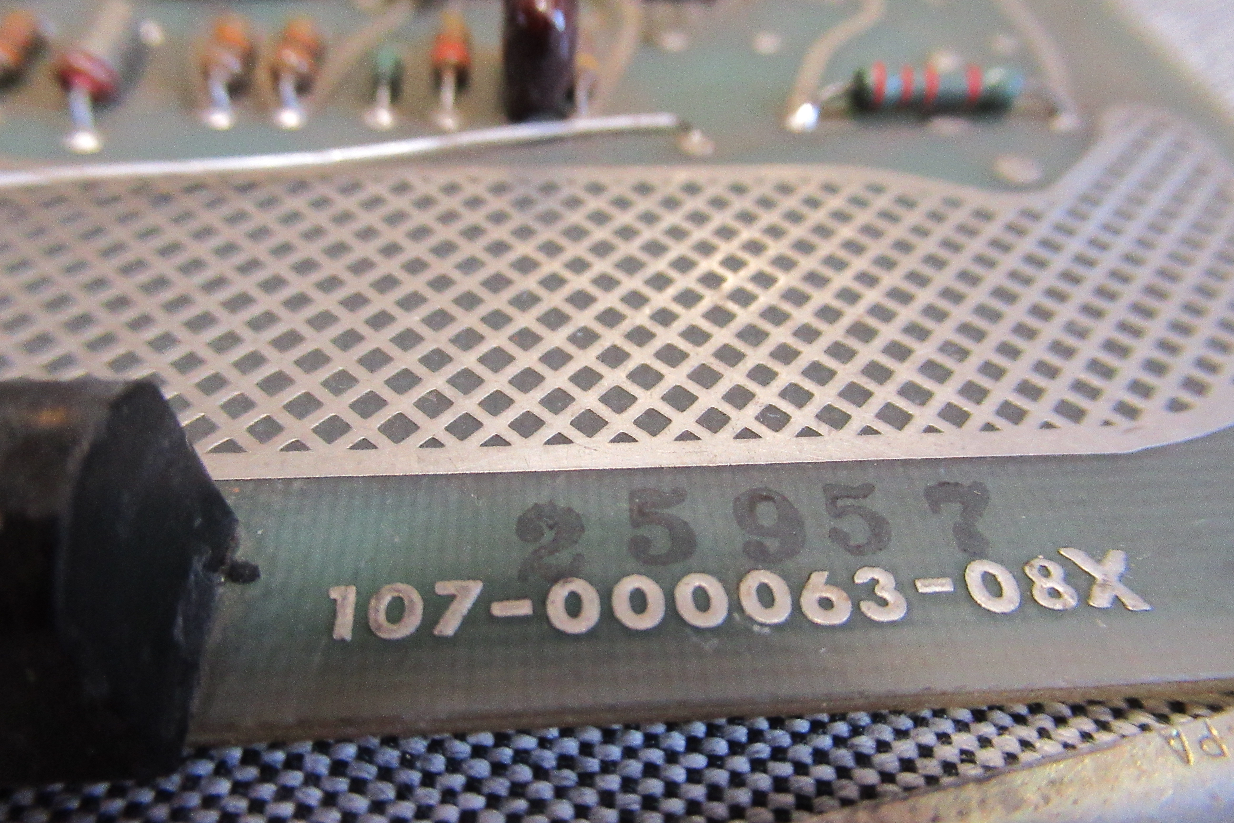
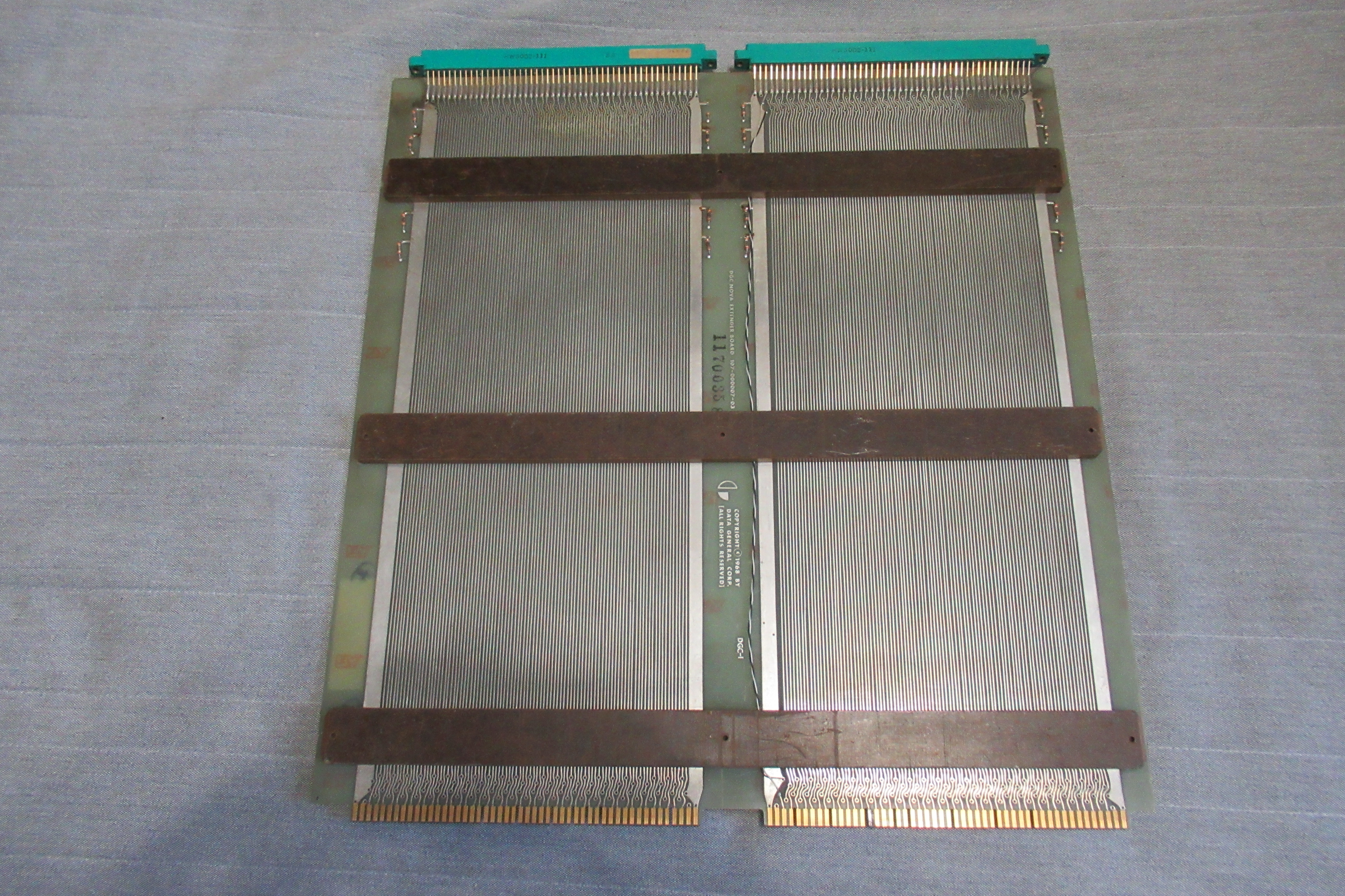
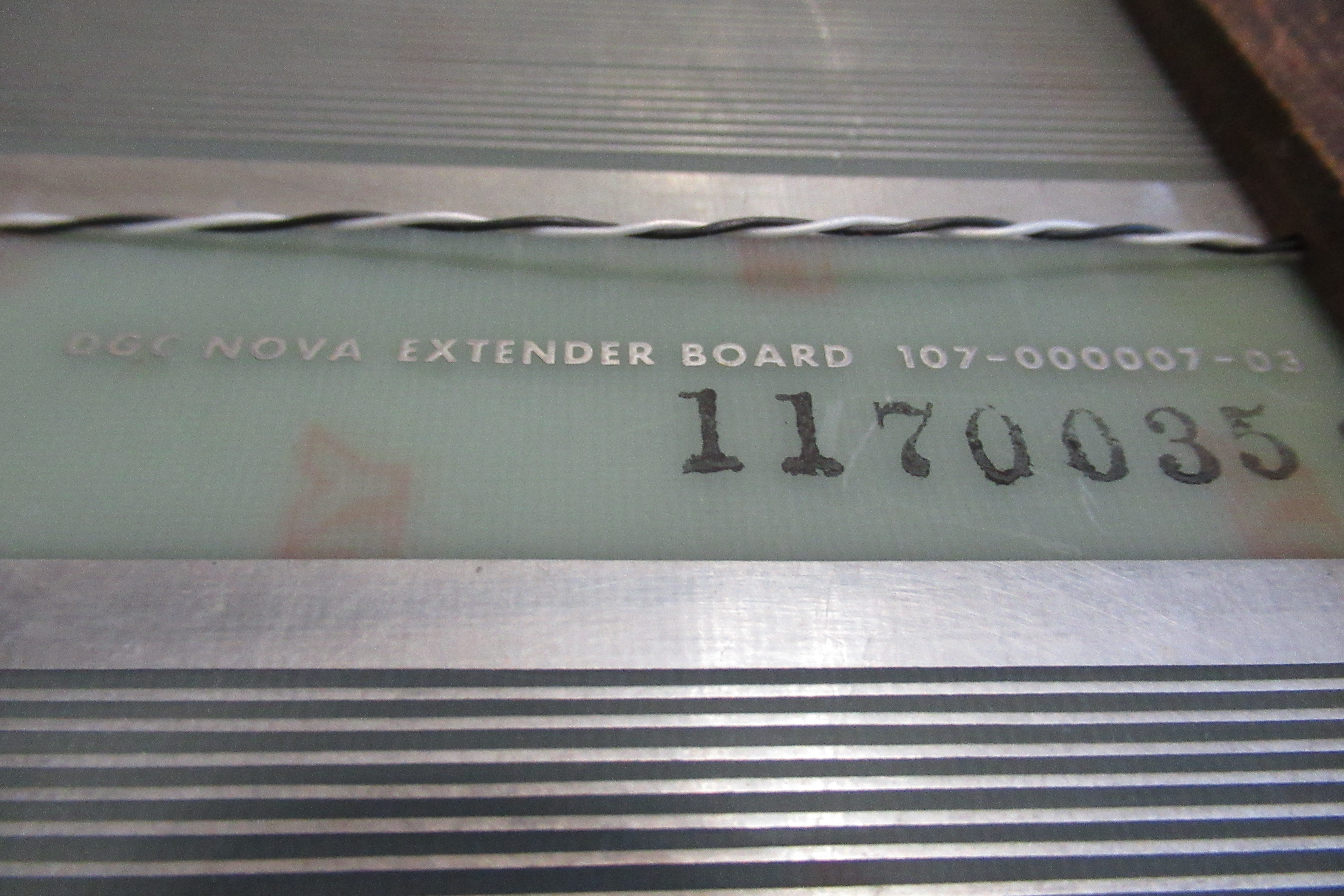
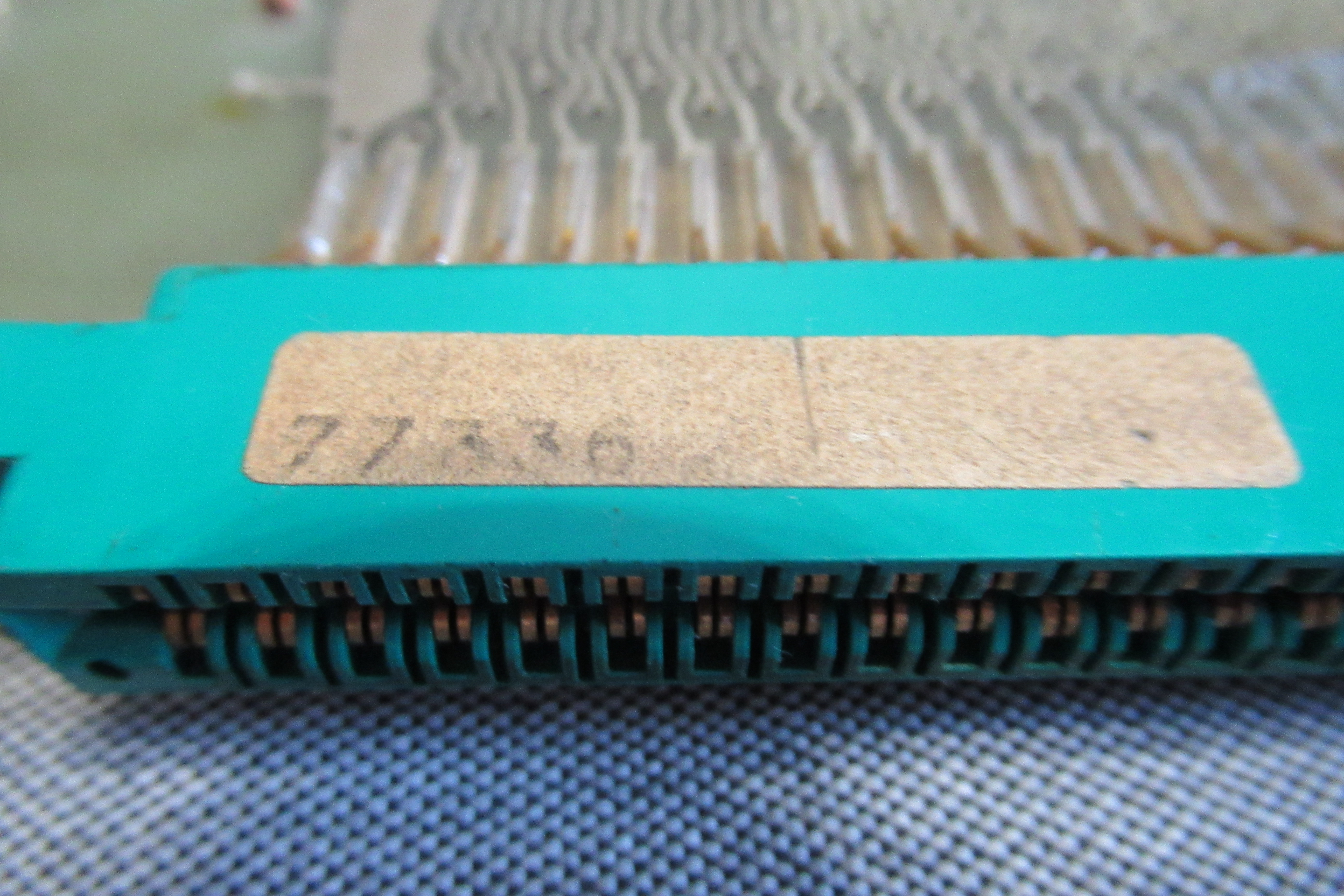
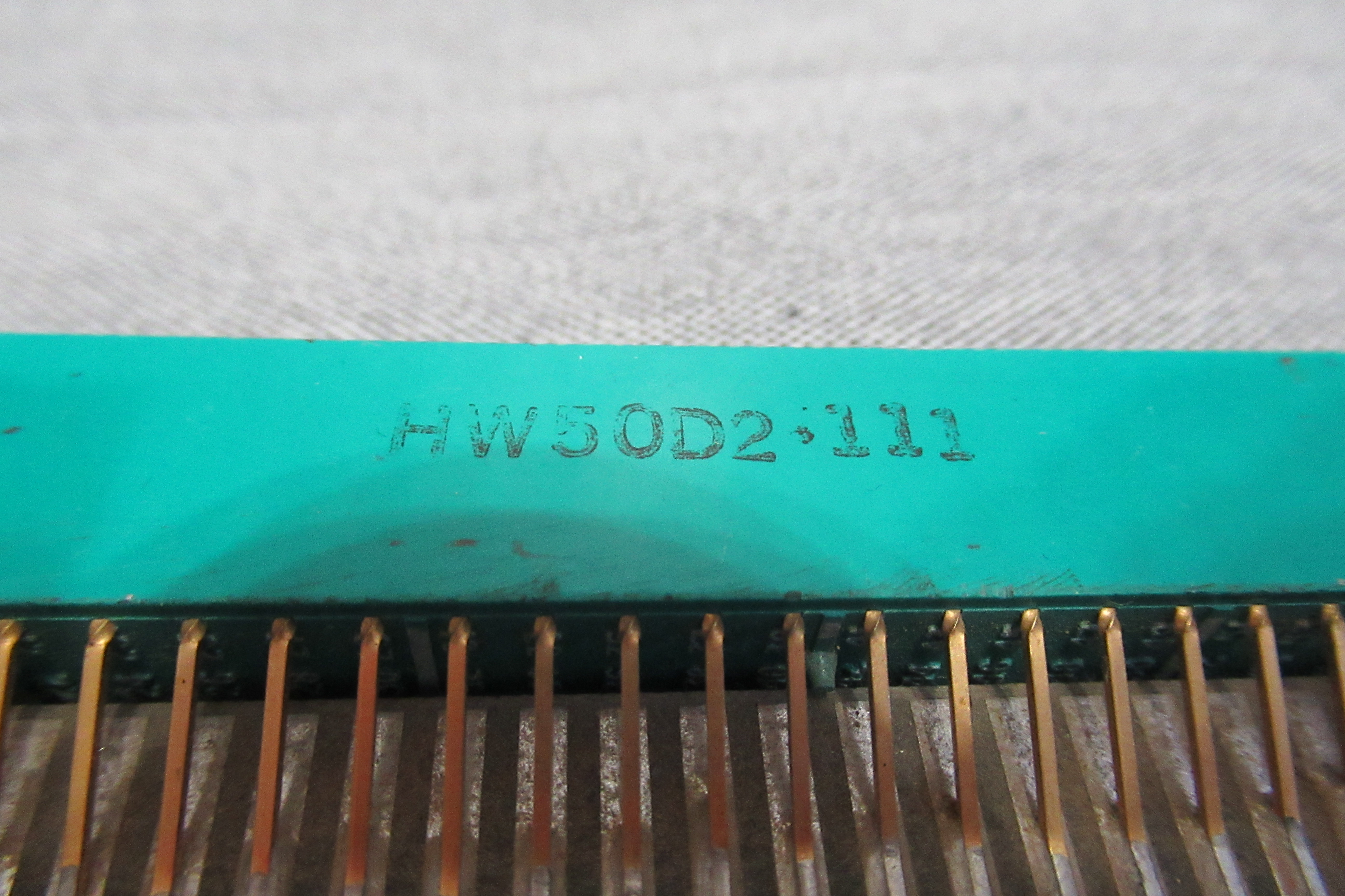
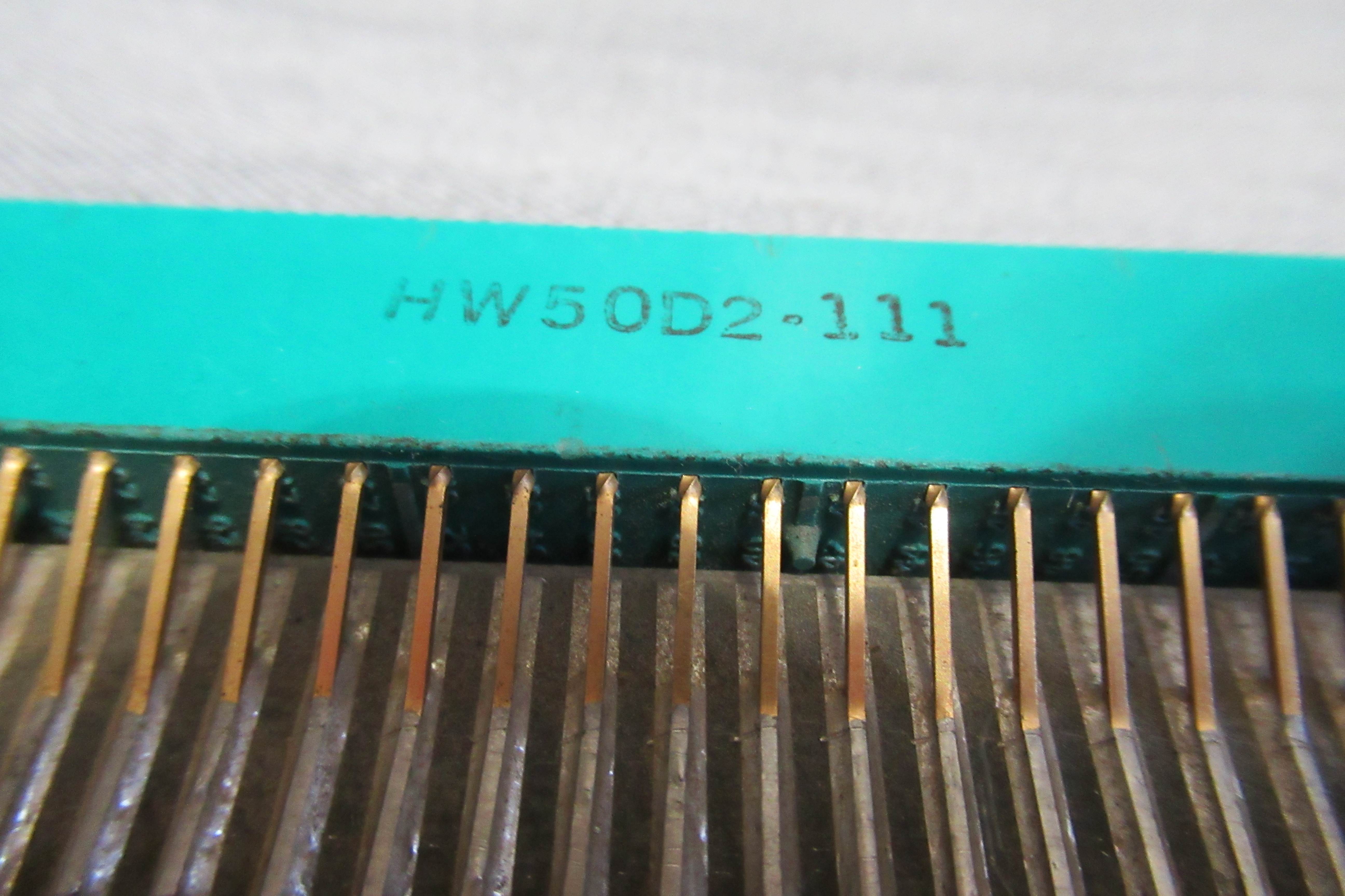
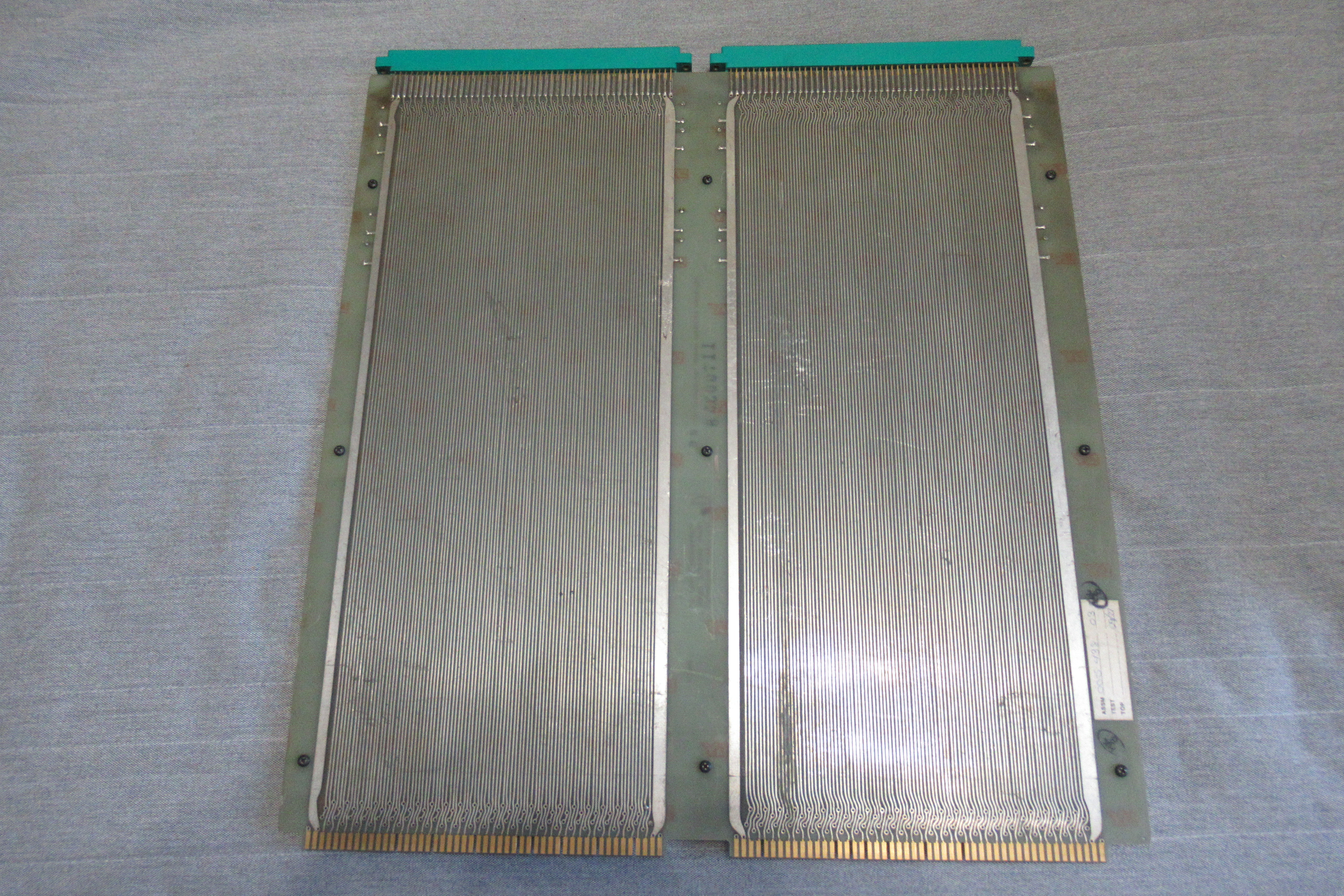
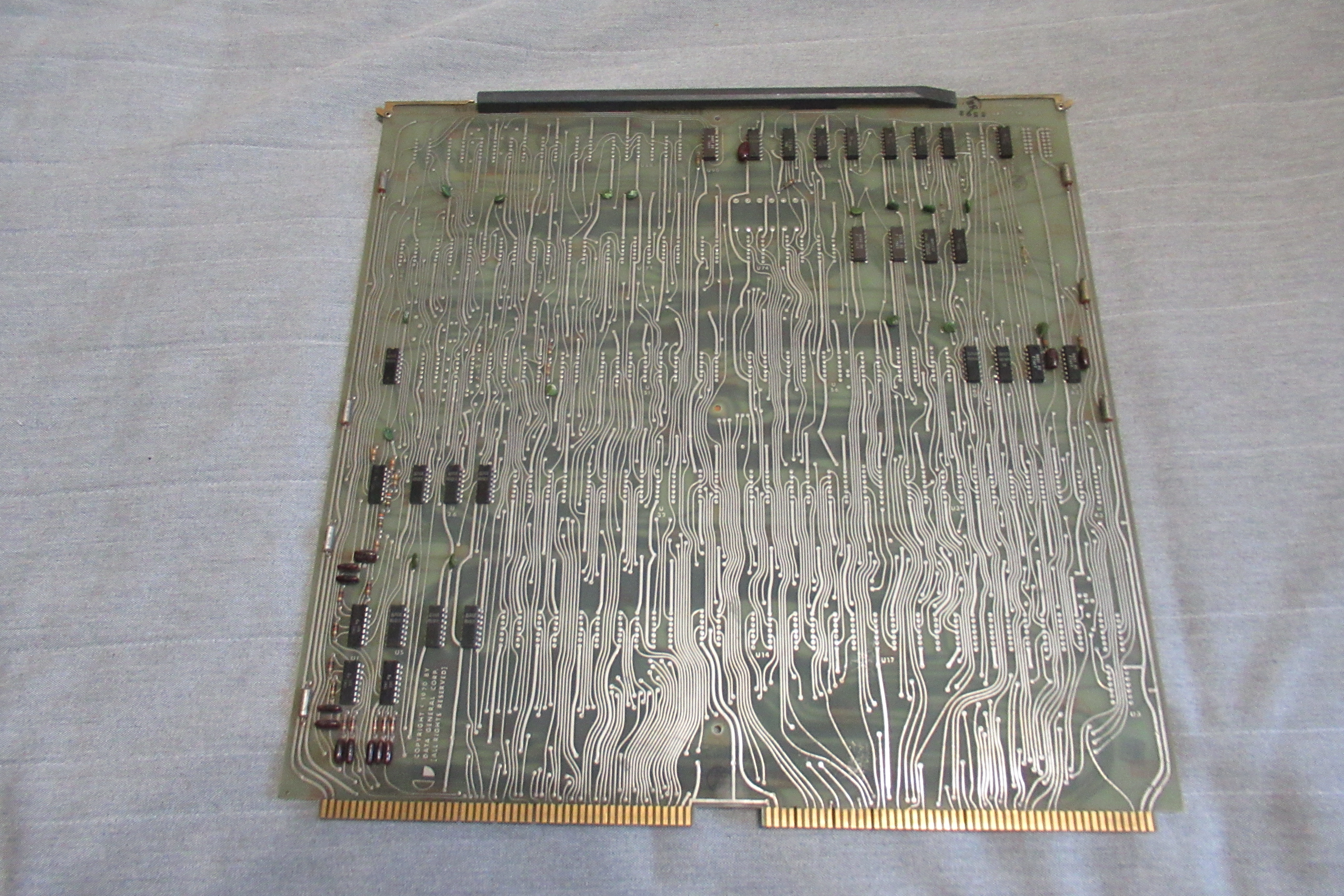
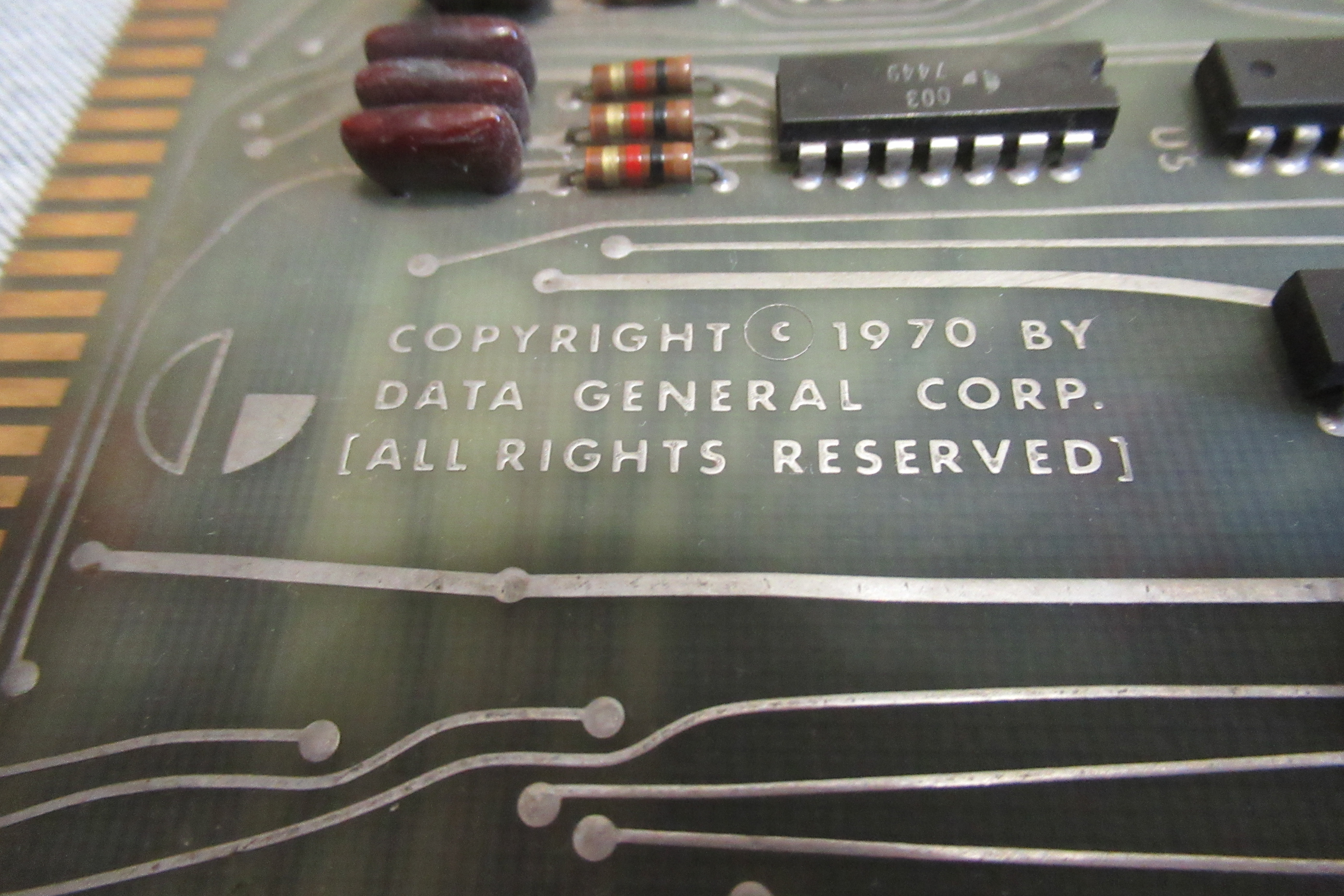
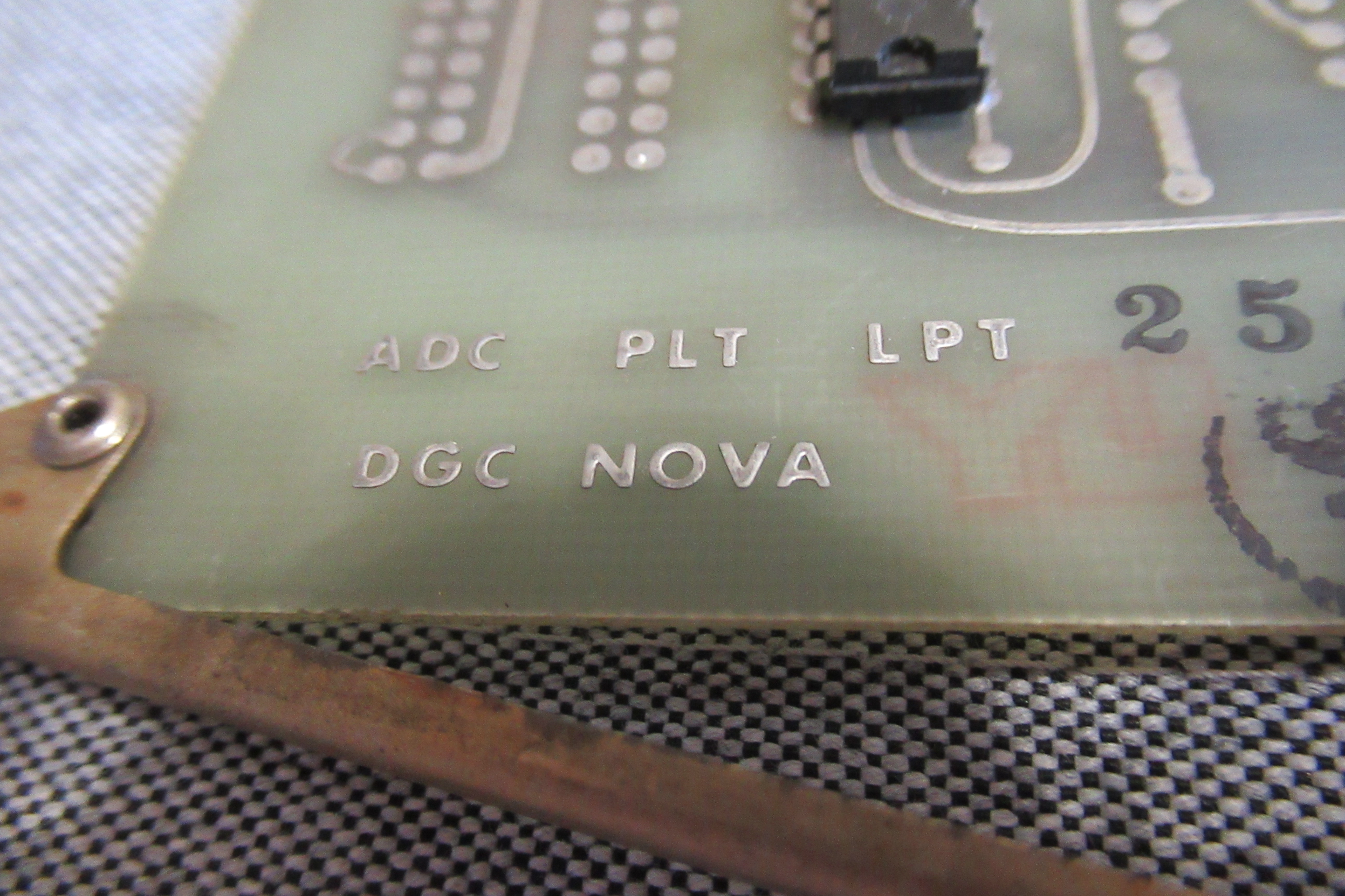
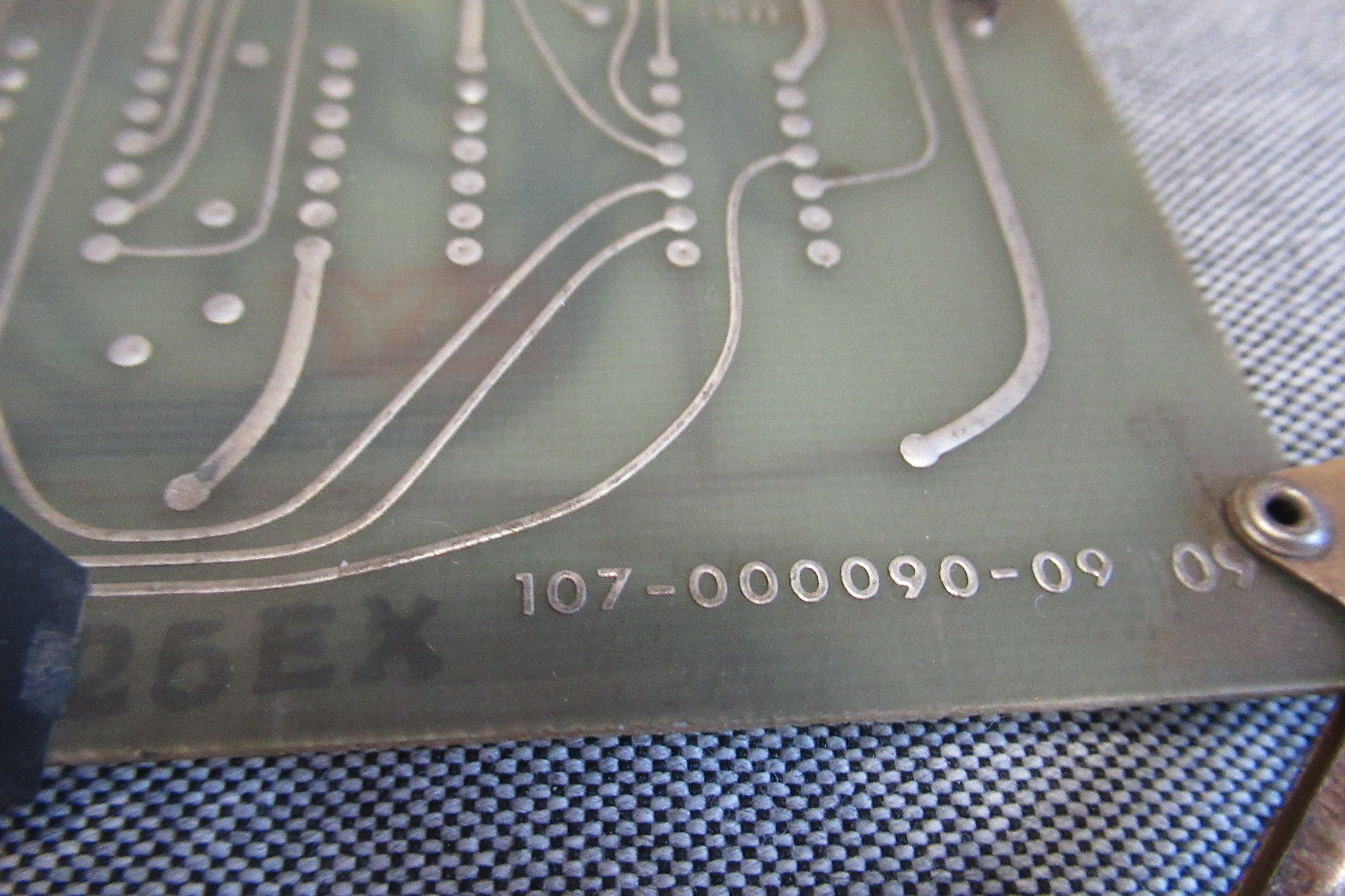
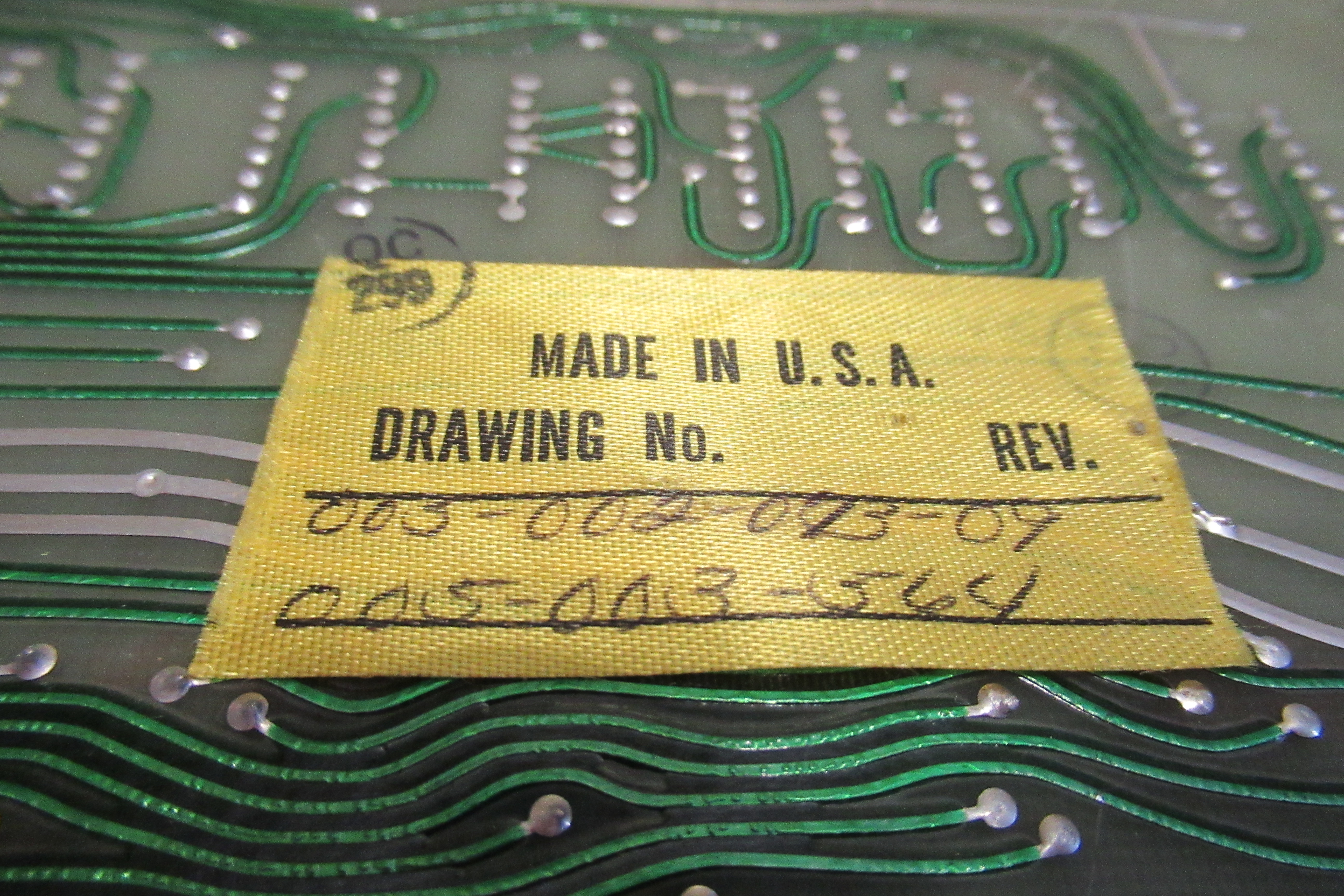
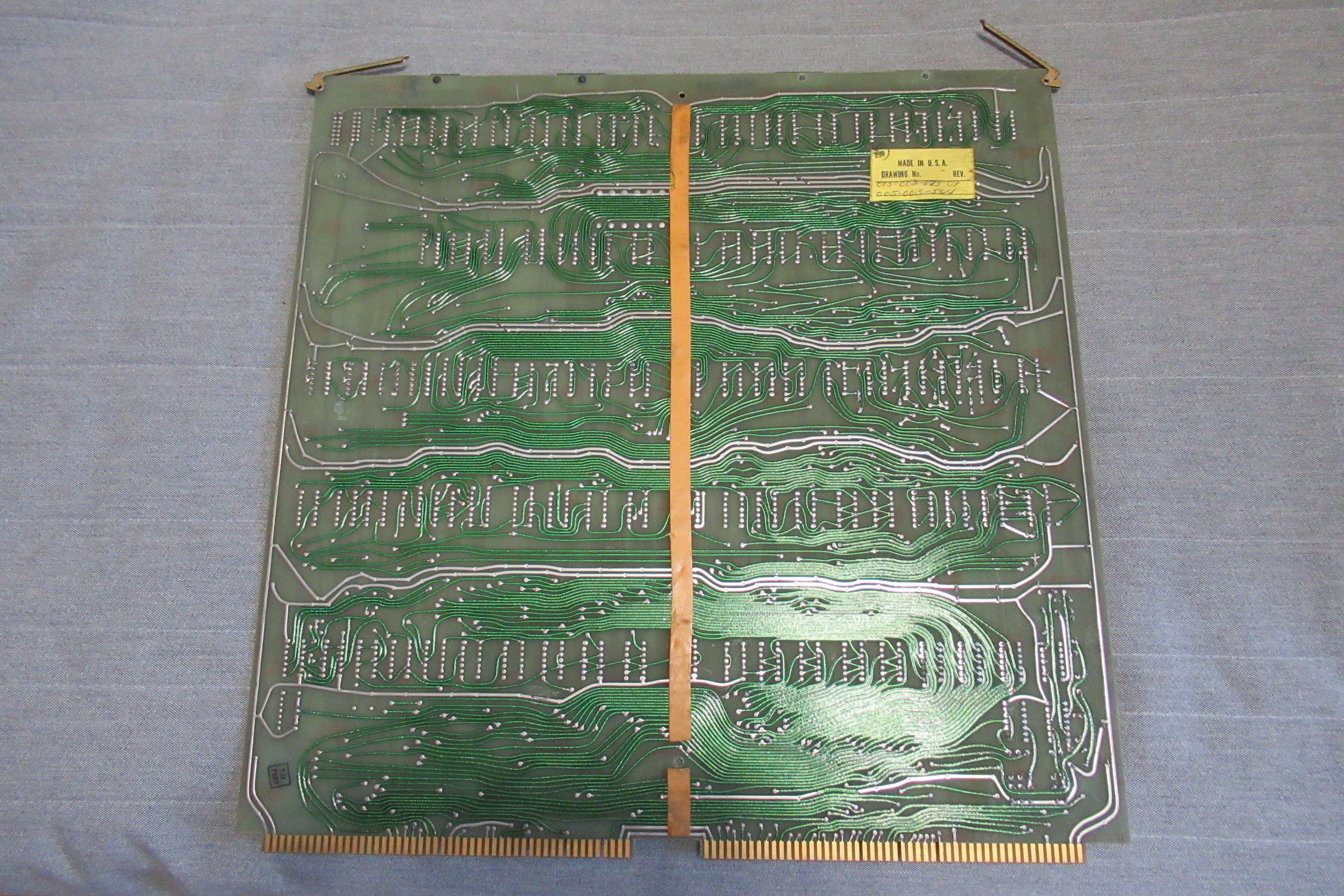
Earlier this year I've bought a bunch of Nova boards seems from different Nova generations (some are marked 1969 and there are definitely later Nova 2 CPUs and core mem).
No chassis neither backplane.
I still want to run it, and considering either to build the backplane myself or buy it (if somebody have extra one).

So, looking for:
- information about backplane signal pinouts (already found it for SuperNova, but is it identical to Nova 2?)
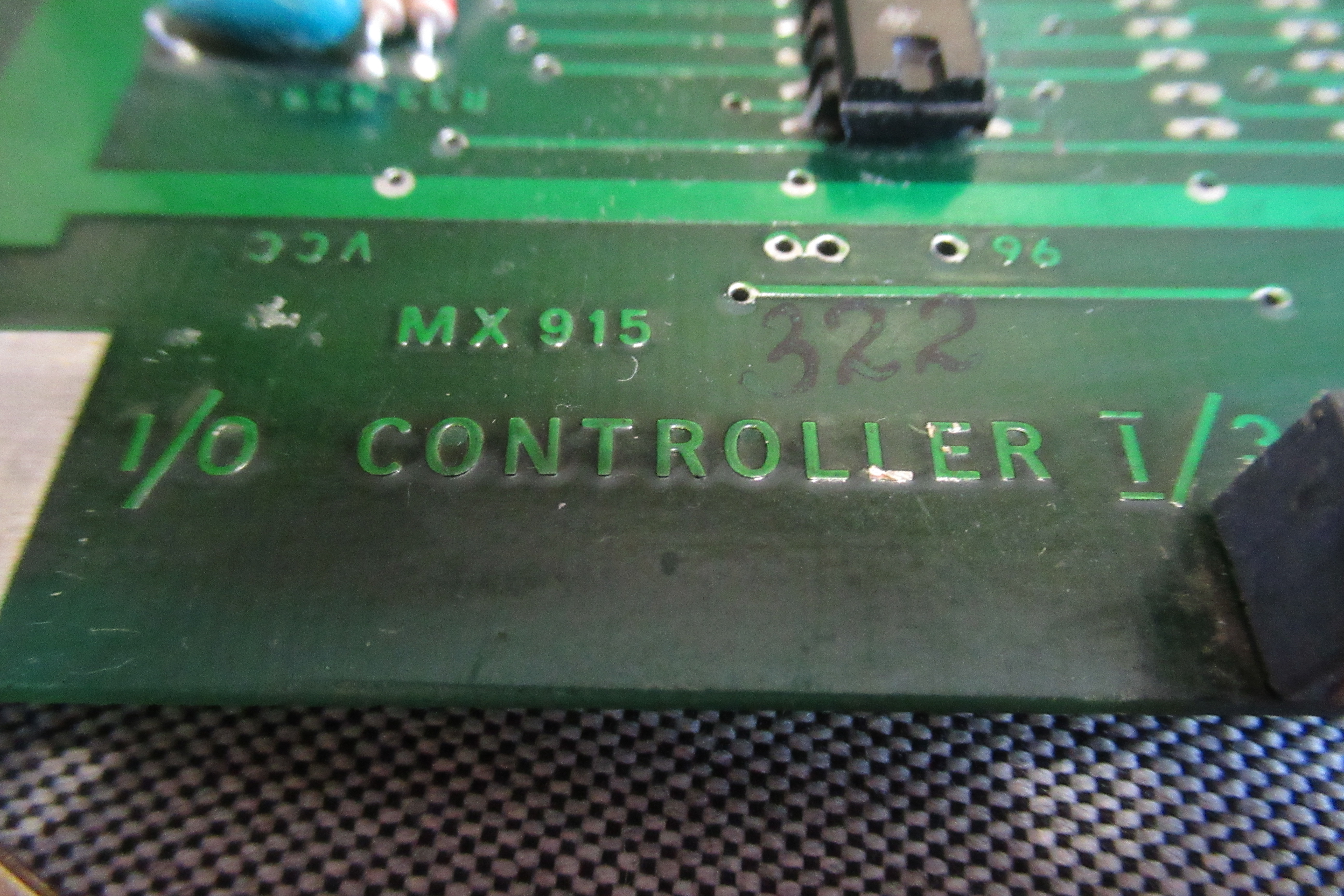
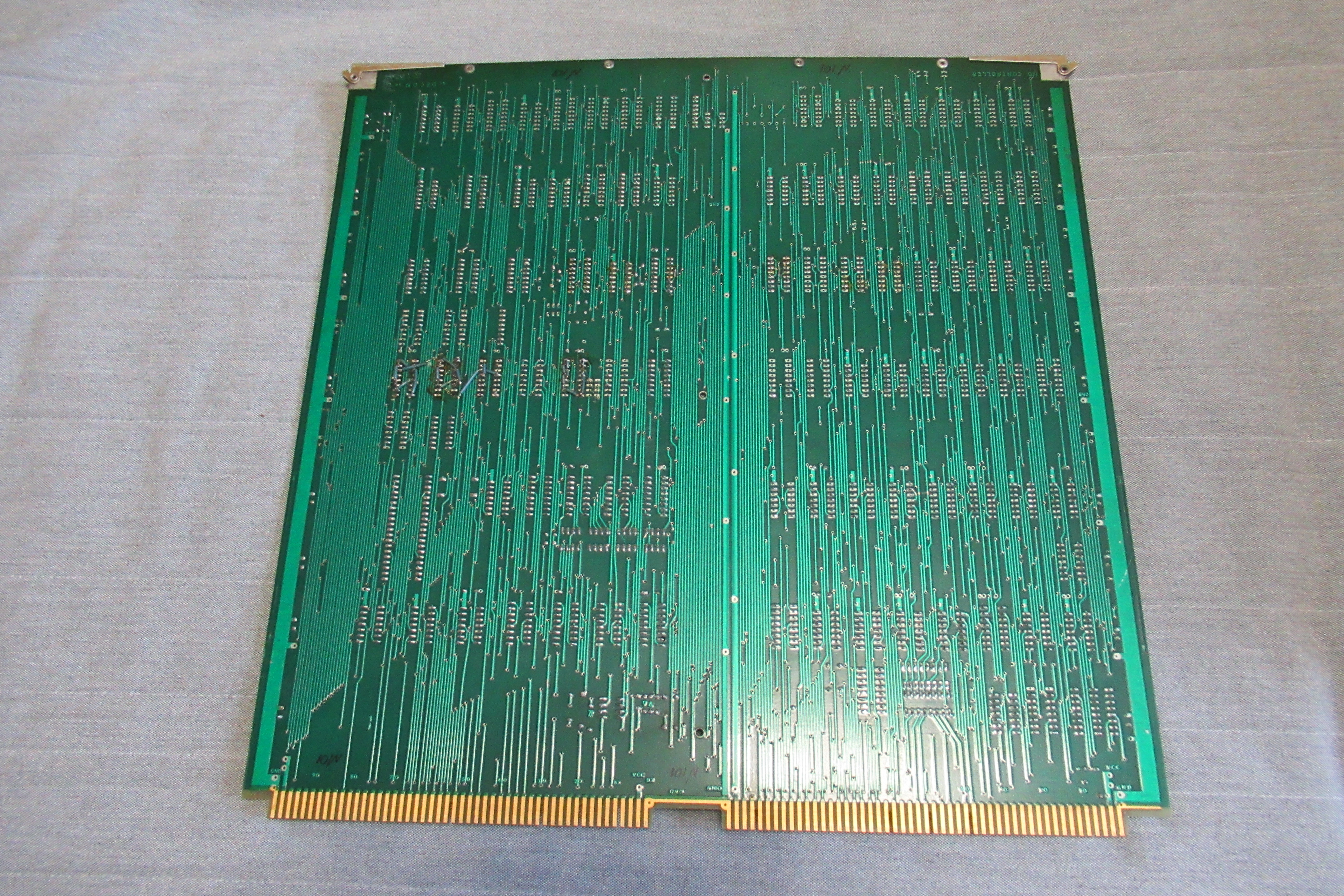
- backplane: option is to buy, or change to Nova 2 CPU, 16k core, also some extra various supplementary boards (I/O, cassete etc)

Thank you very much.
 
Strongly suggest that you start by first listing (in detail) the boards that you have in-hand. DG board numbering is (IMO) incredibly obtuse; you need to collect not only the sticker-type labeling on the primary stiffener, but also the PCB surface markings (copper and/or ink) near both ejectors. Plus any other unique markings. IMO copyright markings are interesting and maybe indicative, but hardly definitive. Obtain a full-board top-side photo with good resolution. Identify large ICs (24-pin and up). Lacking the extensive online documentation of DEC equipment it sometimes requires visual comparisons to other boards to discern relationships and lineages.

As Steve points out the I/O slots are partially bussed (addressing/data/control), whereas the first few slots are wired exclusively for CPU, FPP, and memory. Since the chassis design doesn't support edge-card connectors for peripheral cabling that means that the "bus" slots are actually wired for specific I/O boards and there are special cables used to bring those unique pin-patterns to a suitable rear bulkhead connector using paddle boards (see various pictures on the net).

IMO it would be feasible to wire up a three-board combination (CPU, RAM, I/O) but I don't think that you'll get the I/O that you want without rolling-your-own. IMO minimum I/O would be two serial plus one parallel interfaces -- console, high-speed "file server", and paper-tape. You'll need to build something for the other end of the "file server" connection. The paper-tape interface would be coupled to an MCU-based emulation.

Of course you'll want to build a front panel surrogate :->.
 
Thanks for the replies.
Yes, I already discovered Nova 2 manual. Still I missed the document at the first link, will study it.
I also found somewhat cryptic DG parts reference.

Sure I'm going to photo all boards but it will take time (there are around 15 in total).

Of course you'll want to build a front panel surrogate :->.
I'm more ambitious, unlike fancy DEC front panels with curves and custom keys, Nova is more simplistic) I think it is possible to build the entire chassis and casing and front panel)
 
but do you intend an exact fit-n-finish recreation? Power supply(ies) as well?
I will definitely monitor the trade places for the missing parts. Without it, exact recreation would be too long and too expensive (but not impossible). Power supplies - at the start it would be something modern for sure. Later, maybe.
My approach for restoration is the maximum possible original components; no hesitation for modern replacement when no other way; usage of the modern storage devices for the initial boot. This is the fastest way to deliver the look and feel and sense to the people. Doing the best with the limited capabilities.
 
I was searching ebay for dec stuff and happened to run across what looks like a core memory for a Nova computer, not sure if it's Nova 2 but I'm pretty sure it's Data General. The title of the item is not so good, so it might not be found by people searching for it.
The supplier is Radwell Overstock, a real company in NJ. I recently purchased an item from them... shipped promptly and packaging was excellent.

Would've just scrolled by this item, but many years ago I recall drooling over Nova computers on display at Fall Joint Computer Conferences (FJCC) or National Computer Conferences (NCC). I had to pause and enjoy the image for a bit of nostalgia ;-)
 
Photoed my boards, here we go. Part 1.
Attention, very heavy images under the spoilers!

1641465559.3170033876.img2693.jpg

1641465576.3170033876.img2694.jpg

1641465593.3170033876.img2695.jpg

1641465609.3170033876.img2696.jpg

1641465629.3170033876.img2697.jpg

1641465645.3170033876.img2698.jpg

1641465661.3170033876.img2698.jpg

1641465683.3170033876.img2700.jpg

1641465699.3170033876.img2703.jpg

1641465715.3170033876.img2704.jpg

1641465732.3170033876.img2705.jpg

1641465750.3170033876.img2706.jpg

1641465777.3170033876.img2707.jpg

1641465790.3170033876.img2708.jpg

1641465805.3170033876.img2709.jpg
 
Part 3
1641466144.3170033876.img2724.jpg

1641466160.3170033876.img2725.jpg

1641466175.3170033876.img2726.jpg

1641466195.3170033876.img2727.jpg

1641466210.3170033876.img2728.jpg

1641466229.3170033876.img2729.jpg

1641466245.3170033876.img2730.jpg

1641466263.3170033876.img2731.jpg

1641466294.3170033876.img2732.jpg

1641466313.3170033876.img2733.jpg

1641466327.3170033876.img2734.jpg

1641466341.3170033876.img2735.jpg

1641466360.3170033876.img2736.jpg

1641466379.3170033876.img2737.jpg
 
One of the photos shows a 16k core memory board with the 6.2V Zener diode missing in the burned section of the PCB.

This part of the board is a poor design where 6.2V is generated from 15V through a 30 Ohm 3W resistor and a 6.2V Zener to supply a bunch of 7475 latches which then drive the 75324 X/Y drivers. Unfortunately the DG designers either didn't read the 75324 Application Note (which recommends to use pull-ups on the inputs) or decided they know better, so instead of using pull-ups on the 75324 inputs they bumped up the supply voltage of the 7475s to 6.2V using the resistor & Zener combination which browns or burns every single board over time. I am less concerned with running the latches at 6.2V than with the primitive way of generating 6.2V and the heat generated.

The reason for my post is to warn that without the 6.2V Zener diode you are applying the full 15V to the four 7475 ICs which fries them and likely also kills the hard to find 75324 X/Y drivers.

Tom
 
Back
Top