• Please review our updated Terms and Rules here

Dual purpose M8560 Serial board

From an old PC printer switch I made a box for selecting between 4 serial devices and baudrates from (300 to 36k4) for a PDP11/05 . The baud generator is inside the box is based on a sn74193. With the switch, it is possible to have all 4 devices connected and used in one session. This is quite handy. The serial interface of the 11/05 is not the same as a M8650, but imho quite similar for this concept.

Do you plan to only enable more baudrates? Or are you also willing to change the other jumper settings of the M8650 for different devices (for example: 8n2, the tty jumper for the ASR-33 and so on) on the fly?

Have fun,
Volker
 
GWiley, thanks for the comments.
The first comment on the 12 bit count, I just was not thinking. Just had to change the right counter D3 from zero to one.
The second comment, changed the count enable lines to just a pull up resistor.
The third comment I had to think about for a while. I may not have this correct. I used a NAND of the right carry out (TC) and the right Q0 to control the LOADs. Before the terminal count, both Q0 and TC are zero. Q0 will go high first as the terminal count is achieved, then the next clock pulse will cause TC to go high, thus placing a low on the LOAD. The next clock pulse will reload the initial count. Is that correct?
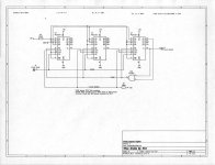
I'm a little anxious to try this, thanks for the help, MikeDivideBy349.jpg
 
GWiley, thanks for the comments.
The first comment on the 12 bit count, I just was not thinking. Just had to change the right counter D3 from zero to one.
The second comment, changed the count enable lines to just a pull up resistor.
The updates look good regarding both of these.
To make the following easier, let's say the '163 chips are numbered U1 on the left, U2 in the middle, U3 on the right.
The third comment I had to think about for a while. I may not have this correct. I used a NAND of the right carry out (TC) and the right Q0 to control the LOADs.
The J? Clock Output should come from U3 pin 14 (Q0) so it is glitch-free. That's the only necessary change.

The updated schematic with the NAND will count as you intend it to do. However, you really only need to invert the U3 TC (pin 15) and feed that back to the load inputs. This is because when U3 TC is one, U3 Q0 will also already be one. U3 pin 14 (Q0) will actually go to one at count 0xf00, decimal 3840. So, the schematic as it is will count in the sequence you want, but only need U3 pin 15 inverted going to pin 9 of all three counters. Q0 is already one when TC is one so no need to and it again.
Before the terminal count, both Q0 and TC are zero.
Before the terminal count, at state 0xffe, 4094 decimal, the Q0 (pin 14) of U1 will be zero, but the Q0 (pin 14) of U3 will have already been one for a while (see above comment).
Inside the '163, TC = T * Q0 * Q1 * Q2 * Q3, so when the counters are cascaded like this with TC connected to T of the next more significant counter, the entire unit works as though you have a single IC that's a 12-bit counter. So, TC of U3 is one only at state 0xfff (decimal 4095).
Q0 will go high first as the terminal count is achieved, then the next clock pulse will cause TC to go high, thus placing a low on the LOAD. The next clock pulse will reload the initial count. Is that correct?
Almost correct.
Code:
Count,    U3-14 Q0,    U3-15 TC,    pins 9 PE/
0xea3        0            0            1    start of the count sequence
0xea4        0            0            1
...etc...
0xeff        0            0            1
0xf00        1            0            1    U3 pin 14 Q0 changes to one
0xf01        1            0            1
...etc...
0xffe        1            0            1
0xfff        1            1            0   U3 pin 15 (TC) to one, PE/ (pins 9) to zero
0xea3        0            0            1    back to the start of the count sequence


I'm a little anxious to try this, thanks for the help, Mike
It looks great and am sure it'll go well.

The simple response:
1. The only necessary change is to connect "J? Clock Output" to U3 pin 14.
2. You can optimize a little by removing the connection between U3 pin 14 and NAND pin 1 but it will still count as intended the way it is.
 
Well..... winter has arrived. Snow cold, wind etal. Even the basement has cooled off. Received the parts I needed to make the new counter. I built my circuit on a bread board and it works! Learned a lot about these chips, 74ls163. They are synchronous binary counters. The new to me feature is that the inputs are sync'ed to the clock. That is to say a clear doesn't do anything until a clock pulse occurs. Same for the LOAD. My counter counts from 3747 to 4096, reloads 3747 and counts again. So optimistically, I wired up a wire wrap board with the same circuit on it and bolted it to the M8560 serial board. Plugged it into the PDP8e and did some measurements. I found that the period at E22 pin 7 was 801.5 nSec or 1.24766 Mc. The board clock seems to be running about 1.5% fast. BUT... the output of the new divide by 349 counter had a period of 415.9 uSec or 2.404 Kc. Should have been 3.575 Kc. So my counter is counting by 519 rather than 349. Well like most circuits I build some trouble shooting is required. First I need to check my wiring. Let you know thanks, Mike
 
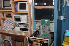
Well, well, well...... success! Things that I tried were checking all the chips, OK, I noticed that on the bread board I just connected all the pull ups directly to +5 volts and I used a 1K resistor pull up on my new board, shorted out the resistor, that did not make a difference. Looked at a bunch of traces on the logic analyzer, the counters seemed to be counting OK, but not by the correct number. I checked all the inputs D0-D3 for the proper initial valve. OK, Then looking at the LOAD pulses, there were way too many. This puzzled me, until I traced the wire wrap. I found that the LOAD connection to the MSB counter was broken. Apparently, when I wrapped this wire the conductor snapped right at the pin and actually looked like it was OK. This connection must have been intermittent and generated the extra LOAD's. After repairing this wiring problem and then struggling with some cabling to get the CIT-101 connected to the PDP8e, the new circuit worked. Here is a picture. The new board is on top of the M8560.
DivdeBy349.JPG
I built the circuit on a large board that I bolted to the top of the M8560. The toggle switch at the top switches between 9600 and 110 baud. The next step is to work with KICAD and see if I can make a small board with my circuit so I can mount the circuit directly over the related circuits on the M8560. I have never ventured past making a schematic with KICAD. Anyway, now is the time. I'm sure I'll have questions on how to make a small PCB board. Mike
 
How should I handle my KICAD questions? Should I ask them here or should I go to the KICAD forum? For example, I want to make this new counter board similar to a raspberry pi shield. Where it just slides on to the M8560 board. That is to say it will connect to the M8560 board via header pins placed in various places. What kind of pins and sockets should I use on both boards? I was looking at some Harwin connector headers, probably single or double pins and sockets. I need 4 data connections, 2 connections for the SPST switch and 2 connections for the +5 power.
I'm also a little confused with assigning the foot prints. For example what does this mean, for a disc capacitor footprint CAPACITORS_THT_DISC_D4.3MM_W1.9MM_P5.0MM?
I think the THT means thru hole type, and the D, W, P are dimensions for the part, but what dimensions? I would guess width and length of the part and wire separation?
Thanks, Mike
 
From here:
I see that D is for Diameter, W for Width, and P is for pad spacing.

I might be some use for board design, but KiCad is new to me too.

Vince
 
Thanks Vince. I've looking over the documentation, but I have a difficult time with text on a computer. I refer books. But either way KICAD is complicated, there is a boat load of stuff to know and consider. I've been looking at you tube films, but seems that the versions I have to the one they are talking about are not the same. The screens did not have the same buttons, but they do sort of piont me in the right direction. I figure I'll just do stuff until I get a PCB layout and then maybe I can print it out on paper to check it. We'll see. Got a lot of reading ahead. Thanks for the help, Mike.
 
This is really close to the needed 220 cps for 110 baud. So, I figured using a 7490, divide by 10, then a JK flip flop divide by 5, followed by a JK flip flop divide by 5. Then with a toggle switched control circuit the would connect the original counters into the circuit for 9600 baud or switch out the original counter for the new 350 counter circuit.
I was looking at the Sol SIT schematic the other day and noticed how they got the 110 baud clock. It looks like they took 1200 Hz and divided by 11 with a (93L16) counter wired to preset 5 on carry. That gets 109.1 baud, which at 1% slow should be close enough.

So divide 9600 by 8 then 11 to get 109 baud.
Bruce, you are probably correct in that the timing only has to right for 11 bits then the timing starts over. So I do not think that 109 or 110 baud would make much difference. Mike
 
I found John Winans' (John's Basement) KiCad tutorial very helpful - though I watched a lot of it at 1.25-1.5x playback speed. Playlist here: https://www.youtube.com/playlist?list=PL3by7evD3F51fKkyrUbH-PCdwPCWc9F8a

Don't be put off by the number of videos - he tends to ramble but discusses a lot of the thought behind his designs and methods.
Jack, I was looking at Shawn Hymel. These were the films I started with when I learned how to make a schematic. John Winan also seems to be pretty good. It's time to start trying this, thanks, Mike
 
The last few days, I have been looking at John's Basement and Shawn Hymel's films on YouTube. Plus some reading on the KICAD document page. I suppose I'm entering the dangerous mode. I know somethings and don't know a lot. Anyway, I have assigned footprints to my schematic diagram. Made a netlist and got my first rat's nest of parts. I pulled it apart and arranged the parts, but then I decided I need to layout where the pins that interconnect the new board to the M8569 should go. Then I discovered I have the wrong footprint for the pins. blah, blah, blah. This caused some start overs. So currently I have decided to measure where these interconnection pins need to go on the M8560 and transfer them to my new board layout. Accuracy is difficult here, since I have to use the M8560 board, rather than a paper print of the traces. So, this weekend I want to make a mach up of the new board with only the pin placements. Then see exactly how they fit to the M8560. I have ordered what I think will be the interconnection pins and sockets. I'm not sure they are correct. We will see when they arrive. Anyway I do not want to drill any holes in my M8560 until I'm sure of what I'm doing. Thanks, have a Happy Thanksgiving, Mike
 
Mike, I appreciate your enthusiasm, but please do us a favor. You say "Accuracy is difficult here, since I have to use the M8560 board,.." Someone with a flakey memory bus adapter on their KL-10 is going to search for info and stumble into this discussion. Please try to refer to your module as M8650 or maybe KL8E if that is easier. Hope you're having an enjoyable Thanksgiving.
 
FTC, sorry. I generally look over the post mostly for grammar and spelling. I have this ability to transpose letters and digits. This has been a problem all my life. I can look at something and see what I want, but it is still wrong. My purpose was to differentiate between the new board and the old board M8650 (checked it). Forgive an old man. Mike
 
Made a netlist and got my first rat's nest of parts. I pulled it apart and arranged the parts, but then I decided I need to layout where the pins that interconnect the new board to the M8650
In this case I think a good component placement on the PCB is like the arrangement of parts on the schematic that you posted. This is often the case. You can rotate the whole thing depending on where you’d like the input and output.

I actually started to make an M8650 baud rate generator board about 6 months ago but didn’t finish it. Planned to use double-sticky foam to attach the module to a small blank space on the M8650, I think it was between the handles and first row of ICs.
 
Gwiley, I've been working on a machup of the connection pins. So far, I have 4 of the 5 set. I had planned on placing 5 sockets and 5 pins to interconnect the new board to the old (M8650). I'm waiting for these parts to come in the mail. While I wait, I'm thinking about which board should get the pins and which should get the sockets. I think I want the sockets on the new board, because I can place their pads on the right side to solder them. I don't have that flexibility with the M8650 board. Getting ready for some family and turkey really soon. Happy Thanksgiving to everyone. Mike
 
So currently I have decided to measure where these interconnection pins need to go on the M8560 and transfer them to my new board layout. Accuracy is difficult here, since I have to use the M8560 board, rather than a paper print of the traces.
The M8650D is fully drawn here:
so it shouldn't be too hard to get a 1:1 PDF of the board drawing.

What I sometimes like to do is to limit the modifications to the original board to installing sockets. Then the original chips can go where they went before, or into the daughter board. If there are enough vias around, you can also just add pin sockets mounted in the vias. That does even less violence to the original board.

The male-male machine pin strips are useful in the daughter board to make the connections, since they fit nicely into the IC sockets.

Vince
 
Back
Top