- VCF South West - June 14 - 16, Davidson-Gundy Alumni Center at University of Texas at Dallas
- VCF West - Aug 2 - 3, Computer History Museum, Mountain View, CA
- VCF Midwest - Sept 7 - 8 2024, Schaumburg, IL
- VCF SoCal - Mid February 2025, Location TBD, Southern CA
- VCF East - April 2025, Infoage Museum, Wall NJ
-
Please review our updated Terms and Rules here
- Forums
- Companies
- IBM Computers, PCs, Clones and Descendants
- PCs and Clones (XT and early AT class machines)
You are using an out of date browser. It may not display this or other websites correctly.
You should upgrade or use an alternative browser.
You should upgrade or use an alternative browser.
How to read parallel-port POST diagnostic codes?
- Thread starter Trixter
- Start date
Chuck(G)
25k Member
Why calculate, when you could just read it?")
Calculate what? If by this time, you can't read 8-bit numbers directly from blinkin' lights, you're not really trying.
Back in the days of RTL, one of my first projects using that logic family was an LED clock--that displayed the time in (binary) HH MM SS (5:6:6 bits).
Trixter
Veteran Member
On M24 I use it with simple flat cable extension, I forgot to tell you.
(facepalm)
My bad. I don't know if I have a straight-through cable, but I'll check.
Edit: Success! Borrowed the cable from a parallel-port ZIP drive, and now I can see my 6300 posts as far at Checkpoint #43h: (DMA timer test OK) but then doesn't get any further. I'm currently disassembling the code that runs between that and the next checkpoint to see if I can figure out a course of action. I'll also dig out a second monitor, as I think the one that came with it is dead.
Edit2: Wasn't able to unearth a monitor, but I did disassemble the BIOS between the two checkpoints better and it is a DMA channel test, along with a test of the first 64K on the system board. I think it is highly likely the RAM test is failing, but I should know for sure once I see the POST text onscreen.
Last edited:
Trixter
Veteran Member
Well, I tested with a known good 6300 monitor, and unfortunately for me, the display card isn't outputting a valid signal, so there is more troubleshooting to be done. But the fact that the LPT codes show the mainboard is indeed executing code is a very hopeful sign, and hopefully with some electronics training on my part, I'll be able to repair what's wrong.
NeXT
Veteran Member
You won't get a video display until later on in POST. If the keyboard LED's just keep blinking you have not even reached the point where the keyboard controller is initialized. They should go out and them almost immediately after you'll get an image.
Also now that I think about this wasn't there something buried in either the AT&T or Olivetti service manual or even the owners manual about the different steps in POST?
Also now that I think about this wasn't there something buried in either the AT&T or Olivetti service manual or even the owners manual about the different steps in POST?
1ST1
Veteran Member
As far as I remember these codes were only available to the electronics workshop at Olivetti where they repaired the boards.
And it's true, you only get message on screen when that POST is finshed. At the moment when BIOS displays something, it also beeps one time.
@Trixter: You need to find out what fails at POST 44h. Have a look at the theory of operations manual, the DMA controller and sourrounding is explained there.
And it's true, you only get message on screen when that POST is finshed. At the moment when BIOS displays something, it also beeps one time.
@Trixter: You need to find out what fails at POST 44h. Have a look at the theory of operations manual, the DMA controller and sourrounding is explained there.
Trixter
Veteran Member
Also now that I think about this wasn't there something buried in either the AT&T or Olivetti service manual or even the owners manual about the different steps in POST?
As it turns out, you're right. The relevant portion in the 6300 Service Manual starting on page 4-10 states the following:
2. The 8086 CPU test is performed. Interrupts are disabled. First, the CPU's status flags are tested using the accumulator and the processor control and conditional control transfer instruction classes. Second, the CPU's general and segment registers are tested with a test pattern. Third, a typical instruction from each of the CPU's data transfer, arithmetic, logical, and string manipulation instruction classes are tested. Fourth, a set of the CPU's addressing modes are tested on ROM. Fifth, the stack segment and pointer registers are initialized to address the ROM stack, and the call/return instructions are tested. Testing the CPU's software-interrupt instruction capability is postponed until after the ROM and RAM modules have been tested. The CPU's hardware-interrupt diagnostics are postponed until after the 8253 real-time clock channel, the 8041 Keyboard peripheral interface, and the 8259 interrupt controller have been initialized and tested, because all three are involved in the testing.
3. The Keyboard peripheral interface chip (8041 or 8741) is programmed and initialized, the lights go off, and a beep is heard.
4. The Display Controller Board is programmed for monochrome 80 by 25 text mode.
5. The parallel printer port and the display are used to report the successful completion of each diagnostic test. The check point bytes are not strobed to the parallel port, so that an attached printer will not confuse the check point information with actual printable data.
6. The parallel printer port and the display are sent confirmation that the CPU test has been successful. If the CPU test fails, an attempt is made to send a "CPU (i8086) Fail" error message to the display, and the CPU is halted.
So part of the POST completes before the display has been initialized, and you only see the codes output via the LPT port. After some components are tested, the display is initialized, the keyboard controller is initialized, and the system beeps. Then the later POST begins, including a full memory test after printing some text onscreen.
@Trixter: You need to find out what fails at POST 44h. Have a look at the theory of operations manual, the DMA controller and sourrounding is explained there.
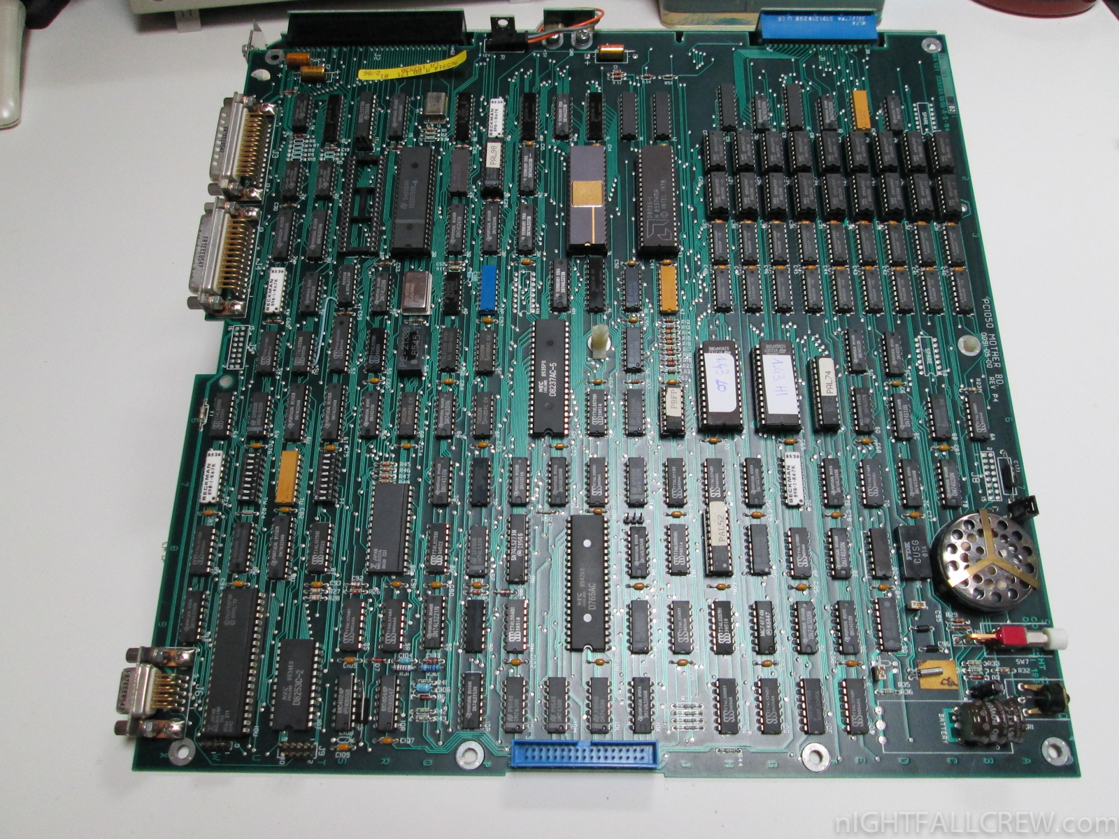
The POST codes output to the LPT port are not documented in any manual I have access to, which is why I've been disassembling and commenting the BIOS POST routines. The last code I see is 43h. Based on my reverse engineering of the BIOS, the code between 43h and 44h tests the DMA channel functionality, and also the first 64K of RAM on the system board.
I don't think it is likely that the DMA channels are faulty, but I do think it is likely that some of the RAM is bad. It looks like the first two banks are 9 x 4164s -- can I locate a bad chip by piggybacking?
Chuck(G)
25k Member
an I locate a bad chip by piggybacking?
Usually you can do that. Every once in a while, it fails to work.
Trixter
Veteran Member
There were some very strong piggybacking opinions both for and against in this thread a year ago. If no chips have obvious shorts (are hot to the touch), and piggybacking is not reliable, then what do most people usually do after that? Replace all the RAM with sockets and swap in known good chips, or is there a more elegant way to diagnose bad 4164s?
gslick
Veteran Member
Are the BIOS ROMs/EPROMs in sockets? Could you write your own memory diagnostics and burn those into your own EPROMs and output your own diagnostic code to indicate which bits are bad if your diagnostics are able to determine that?
That might be a more fun project from my own point of view than breaking out a soldering iron to unsolder and socket a bunch of DRAM chips.
That might be a more fun project from my own point of view than breaking out a soldering iron to unsolder and socket a bunch of DRAM chips.
Chuck(G)
25k Member
Well, since the 6300 is an 8086 box, does anyone have a spare ICE to lend?
There's always the logic analyzer route as well.
If the suspicion is that the first 64K bank is bad, then insert your own POST code if the test fails.
There's always the logic analyzer route as well.
If the suspicion is that the first 64K bank is bad, then insert your own POST code if the test fails.
gslick
Veteran Member
I have a Fluke 9010A and I'm pretty sure I have an 8086 probe for it. That would probably the quickest way to check for a memory problem.
I also think I have an HP 8086/8088 processor probe for HP logic analyzers which could be used to trace the BIOS execution flow.
I also think I have an HP 8086/8088 processor probe for HP logic analyzers which could be used to trace the BIOS execution flow.
NeXT
Veteran Member
Well, since the 6300 is an 8086 box, does anyone have a spare ICE to lend?
There's always the logic analyzer route as well.
My progress on troubleshooting my machine is documented somewhere here on the forum.
When I had my HP 1600A hooked up to both the CPU and the EPROMs (which ARE socketed) I could see that there was something happening while synced to the system clock and it responded to a RESET but I could never determine exactly what it was doing. My analyzer is far too old to sample more than a few lines of data at a time so I couldn't see if I'm actually seeing it stuck in a loop or if it's just garbage data being pushed around.
The biggest problem with these boards is half the ram is socketed.
In theory if you disregard the ram piggybacking discussion you could disable the second bank and use it to piggyback the other bank but in my machine this failed to yield any changes.
Last edited:
There were some very strong piggybacking opinions both for and against in this thread a year ago. If no chips have obvious shorts (are hot to the touch), and piggybacking is not reliable, then what do most people usually do after that? Replace all the RAM with sockets and swap in known good chips, or is there a more elegant way to diagnose bad 4164s?
I generally remove the 4164s, install sockets, put the old desoldered 4164s in the sockets and replace them one at a time.
I like to do that in most cases as soon as there is a RAM problem; I like to have sockets at that point, but that's just me.
If you'd like, being that you're in relatively close proximity, I could install sockets for you. I wouldn't try to save the original chips though. I just don't have the time and space for a big project. But I can cut chips out and install sockets even away from my bench and still end up with a professional job.
I generally remove the 4164s, install sockets, put the old desoldered 4164s in the sockets and replace them one at a time.
I like to do that in most cases as soon as there is a RAM problem; I like to have sockets at that point, but that's just me
Yup me too, I'm not that much of a stickler for authenticity when it comes to fitting sockets where there originally was none, Though removing a chip complete can be a right pain in the arse sometimes.
1ST1
Veteran Member
That is what I told you above. Parallel port POSt codes come before monitor init. It beeps and then BIOS message on the monitor comes up.As it turns out, you're right. The relevant portion in the 6300 Service Manual starting on page 4-10 states the following:
So part of the POST completes before the display has been initialized, and you only see the codes output via the LPT port. After some components are tested, the display is initialized, the keyboard controller is initialized, and the system beeps. Then the later POST begins, including a full memory test after printing some text onscreen.
The POST codes output to the LPT port are not documented in any manual I have access to, which is why I've been disassembling and commenting the BIOS POST routines. The last code I see is 43h. Based on my reverse engineering of the BIOS, the code between 43h and 44h tests the DMA channel functionality, and also the first 64K of RAM on the system board.
I don't think it is likely that the DMA channels are faulty, but I do think it is likely that some of the RAM is bad. It looks like the first two banks are 9 x 4164s -- can I locate a bad chip by piggybacking?
I am not sure if t is memory. But you can piggyback 4164, that should work for testing.
Trixter
Veteran Member
Thanks to this conversation, I have learned a few things:
- Piggybacking doesn't always work, but if it does, it saves a lot of time
- Things like the Fluke 9010A exist (do those kinds of "emulate a CPU" boxes have a standard name? It's like an ICE, but not like an ICE...?)
- A hardware ICE would let me trace execution, but those seem to be as rare as hen's teeth
- A logic analyzer could help me if I understood how to use them (I am researching this)
Unfortunately, the piggyback test of the first 64K didn't change the behavior; I did each of the 9 chips in the first bank individually, then all 9 simultaneously, both without success. So either the RAM is still actually bad, or the 8237A-4 DMA controller chip is bad since that's also what is being tested in that part of the POST. So my next question: How often does a DMA controller go bad vs. the RAM itself? Is it a common operation for an 8237 to go bad and need replacement?
(I understand that a broken trace on the motherboard could also exhibit these problems; I'm just exploring what is within my capabilities first.)
They are, and that indeed would be a cool project! I don't know how to work with EEPROMs (there are two of them, I'm guessing one is the even bytes and the other is the odd bytes?), but I do know x86 assembly.
I had the same experience.
How do you get the clipped legs out without access to the other side of the board?
- Piggybacking doesn't always work, but if it does, it saves a lot of time
- Things like the Fluke 9010A exist (do those kinds of "emulate a CPU" boxes have a standard name? It's like an ICE, but not like an ICE...?)
- A hardware ICE would let me trace execution, but those seem to be as rare as hen's teeth
- A logic analyzer could help me if I understood how to use them (I am researching this)
Unfortunately, the piggyback test of the first 64K didn't change the behavior; I did each of the 9 chips in the first bank individually, then all 9 simultaneously, both without success. So either the RAM is still actually bad, or the 8237A-4 DMA controller chip is bad since that's also what is being tested in that part of the POST. So my next question: How often does a DMA controller go bad vs. the RAM itself? Is it a common operation for an 8237 to go bad and need replacement?
(I understand that a broken trace on the motherboard could also exhibit these problems; I'm just exploring what is within my capabilities first.)
Are the BIOS ROMs/EPROMs in sockets? Could you write your own memory diagnostics and burn those into your own EPROMs and output your own diagnostic code to indicate which bits are bad if your diagnostics are able to determine that? That might be a more fun project from my own point of view than breaking out a soldering iron to unsolder and socket a bunch of DRAM chips.
They are, and that indeed would be a cool project! I don't know how to work with EEPROMs (there are two of them, I'm guessing one is the even bytes and the other is the odd bytes?), but I do know x86 assembly.
In theory if you disregard the ram piggybacking discussion you could disable the second bank and use it to piggyback the other bank but in my machine this failed to yield any changes.
I had the same experience.
I can cut chips out and install sockets even away from my bench and still end up with a professional job.
How do you get the clipped legs out without access to the other side of the board?
AmigaJules
Experienced Member
How do you get the clipped legs out without access to the other side of the board?
I clip the the chip out completely from the component side, then heat the pin from the solder side, grab it with tweezers from component side and pull it out.
Then a little work with the solder sucker to clean out the holes and it's ready for sockets.
But I do it on a bench...
1ST1
Veteran Member
Sometimes I should have a closer look to my harddisk, to what I have collected there...
View attachment 34180
View attachment 34180