• Please review our updated Terms and Rules here

I wish to create a new DMA/RAM expansion card for the Tandy 1000 line.

If you're up for fooling with your breadboard setup, here's something we could try. Here's the Tandy Faxback that mentions the 768k configuration for the 1000 HX when equipped with the 25-2062:

ftp://ftp.oldskool.org/pub/tvdog/tandy1000/faxback/01083.pdf

I can't find a schematic or manual for that board, so the two possibilities are:

1: That board is just 512k in a linear array, nothing special, and the software it comes with tweaks the Big Blue mapper to enable using the extra memory that's present but otherwise hidden in this configuration, or:

2: That board has a mapper on it that sticks its extra RAM in a UMB or banks-switches it.

If it's possibility #1, then in principle you might be able to run the RAMdisk driver that's compatible with the Tandy board with your breadboard setup. This looks like the right driver:

ftp://ftp.oldskool.org/pub/tvdog/tandy1000/utilities/mempdrvr.exe

It's worth a shot?
 
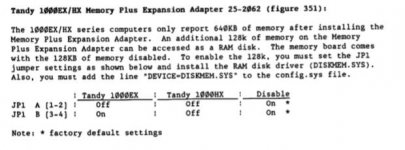
... still failing to find a detailed theory of operations for the 25-2062, but I did find this which makes me suspect that the RAMdisk driver isn't going to work with the "jumpered straight across" setup. (It's still probably worth a try just to make sure.)

Screen Shot 2019-06-14 at 1.39.04 PM.jpg

That it has different jumper settings for the EX and HX suggest that it could be mapping that 128k into the UMB areas, because EX and HXs have different areas that are open. (If the manuals are to believed the EX has everything from C000h to EFFFh open, while the E-page is occupied by DOS in an HX.) Wish someone had one of these cards to run Check-It on. If it is using UMBs it'd be neat to know *which* it uses.

Anyway, *If* that's the case then I think we can give up on hopes of easily getting "free RAM" in the A-page or eliminating the video page steal from conventional, but that's fine, it's a Tandy 1000 and that's the cost of admission. The question is still then what's happening with the straight-across jumpered setup counting to 640k and working. The wording of the manuals do suggest it could be counting up, seeing that there's 512k of expansion memory, and based on that it's loading the BB register with the value set that says "Map at 8FFFFh, and Big Blue RAM == 128k", therefore disabling 128k of the built-in RAM. The other possibility is the BIOS is loading for the 384k/256k split and 128k is conflicting but it's not caring. Again, it would be really nice to be able to tell for sure which.

The safest route if we can't figure out if contention is definitely *not* happening is to limit to 384k of the SRAM. If we're going for the ultimate in minimalism... I think you could do it with a single 74LS00? (Logic: one NAND gate across A18 and A17, that will give you a "1" for every condition but 11. Use a second to invert A19, that'll give you a 1 when you're in the bottom 512k. Then use a third gate to combine those two, that'll give you a "0" for enable when A19 is low *and* you're in the first three 128k pages of the SRAM chip.) That's a three-chip conventional backfill board *including* a '245 buffer.
 
Last edited:
This is a surprise. I had no idea they had a 512K board!

The safest route if we can't figure out if contention is definitely *not* happening is to limit to 384k of the SRAM. If we're going for the ultimate in minimalism... I think you could do it with a single 74LS00? (Logic: one NAND gate across A18 and A17, that will give you a "1" for every condition but 11. Use a second to invert A19, that'll give you a 1 when you're in the bottom 512k. Then use a third gate to combine those two, that'll give you a "0" for enable when A19 is low *and* you're in the first three 128k pages of the SRAM chip.) That's a three-chip conventional backfill board *including* a '245 buffer.

That would be my ideal setup anyways. No frills, straight "plug and play" memory expansion that people wouldn't have to worry about. Most people won't have any idea of what to do with UMB anyways.
I don't have a '00 on hand (add a couple of those to my next Digi-Key order to have on hand), but I'll see if I can kludge something else together.
 
That idea of using NANDs was the first thing I could think of to do decoding with one chip (not counting programmable logic). A '138 or '139 plus an '08 or similar is the easy two chip solution.

Did you try running the RAMdisk driver on the jury-rigged system just for laughs? Now that I was finally able to dig up the fact the original 512k board had those jumpers on it I'm not optimistic, alas, but it still might be worth a shot just to make sure.

I'm still waiting for all my from-China goodies but I did get the extra-tall Raspberry Pi stacking headers yesterday. There's good and bad news on that front:

Good: a set of them stacked together has essentially identical spacing to the Plus slots. If I stick a set on my modem card it rests perfectly in the middle slot position when the stack is inserted into the EX.

Bad:

Apparently I misunderstood, at least on the headers I bought the "xtra tall" spacer plastic can't be moved. As a result any board using this idea is going to rest *really* close to the bottom of a real Plus card stacked on top.

Also, I apparently completely wiffed on the fact that these 2xXX headers aren't designed to fit snugly together, so in addition to having to cut one header down from 2x20 to 2x11 I had to file most of the wall off the cut end to make it fit the pin spacing. It works but, man, I wish 62 pins were a standard size.

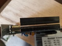
Also, possibly important data point: maybe the modem card is an outlier, but from actually extracting it I can say that you might need to leave a "gutter" almost one inch deep on the component side to be absolutely sure of no interference. See how this transformer essentially rules out fitting this card on stacked headers at all.

20190615_123157.jpg

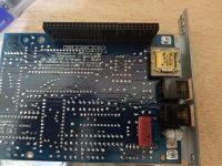
And another shot of the bottom of the modem card.

20190615_123316.jpg
 
I haven't had a chance to test the mem driver til this morning, I've been using my spare time to work on maintenance on my ride-on mower for the past couple days (I'm a landscaping contractor, this stuff is just my hobby).
Results of DEVICE=DISKMEM.SYS says that Upper Memory is not enabled, disk not installed.

So that's a no-go without more info on that 512K card.

I'm placing a Digi-Key order for a couple '00's to test limiting this to 384K , as well as some other supplies I need, including a larger breadboard that'll be handy going forward (much easier to prototype concepts on a breadboard than a perfboard). Should be here in a couple business days. If your '00 idea works, we should both be able to commit to a 3-chip minimalist design for the memory portion of our respective cards.

Hey, since you have the modem card, could I confirm some measurements with you (with calipers, if you have them)? I've figured the rough measurements for the template that I'll be using going forward with these PLUS cards (based on the Tandy DMA/RAM card), and your modem card will allow me to confirm before I commit this template. It would probably be a good idea to use decimal inches (as much as I prefer metric, this system was laid out based on decimal inches).
The origin reference I prefer to use is pin 1 on the PLUS header (NMI or I/O check), which is a constant across all PLUS boards relative to the middle of the 3 holes so near as I can tell.

a. spacing between the three holes on either side. Should be about 0.235", based on the spacing between the headers on the Tandy DMA/RAM card.
b. overall width and height of the bracket.
b. between the outside of the bracket and the furthest inside edge of the transformer (the gutter looks to line up with header pin 1, which is what I had figured anyways, about 1.07" from the outside).
c. distance at right angle between pin 1 and the nearest centre hole, which I figure to be about 0.54"
d. between the component side of the board (the inner-side of the mounting tab), and the centre line of the 3 holes. I get about 0.300"

If we're accurate to within two decimal places, it should be sufficient.
 
I haven't had a chance to test the mem driver til this morning, I've been using my spare time to work on maintenance on my ride-on mower for the past couple days (I'm a landscaping contractor, this stuff is just my hobby).

Yeah, sorry if I sounded like I was pestering. (Believe it or not designing old Tandy boards isn't my full time job either, just my current "hey, let's do this because reasons!".) ;) Just hoping you'd see and get a chance to run the test before pulling apart your breadboard setup, if you hadn't already because, you know, data.

Results of DEVICE=DISKMEM.SYS says that Upper Memory is not enabled, disk not installed.

On one hand that's disappointing, because I was *really* hoping how that board worked was setting the bottom of the Big Blue RAM as 512k and using the A-page and the first 32k of B for the RAM disk because it would have made getting that extra memory basically completely "free". But on the other it's nice that the driver unambiguously said that it's using upper memory blocks to provide it, so the only remaining mystery is *where* it would map that memory. I have theories which boil down to it probably being D000-EFFFh on an EX and C000-DFFFh on an HX. Which if true would imply an HX couldn't have the extra memory enabled if you had any kind of board installed that used a BIOS extension. Or maybe you only get 64k on an HX?

(That snippet I did find said the extra RAM is disabled by default, so not knowing how rare the card is it's possible a lot of people who had one *might* have had no idea it had that special feature if someone else installed it for them. It'd be *really* nice to either have the manual or find someone who has a machine with it installed and enabled willing to run Check-it! or the like.)

I'm placing a Digi-Key order for a couple '00's to test limiting this to 384K , as well as some other supplies I need, including a larger breadboard that'll be handy going forward (much easier to prototype concepts on a breadboard than a perfboard). Should be here in a couple business days. If your '00 idea works, we should both be able to commit to a 3-chip minimalist design for the memory portion of our respective cards.

I spent a few minutes on Sunday pasting together an update to my combo RAM-ROM-Calendar card reflecting the likely new reality. With the flash/calendar I need to add a 74138 to cut the C000-FFFFh space into 32k chunks (I'm trying to be slightly clever using the NAND gate left over on the '00 to let me get 32k resolution) and a 7408 AND gate to combine chip selects to drive the single '245 buffer, and an idea did hit me for how to enable a 64k UMB with little effort using a couple unused gates on the 08. Unfortunately it'd be at E000h so useless on the HX. You could shuffle the last 64k page of the RAM chip to D000h by selectively inverting the a17 address line when a D000 page select is active, but I haven't had enough coffee to think of an elegant way to do that doesn't add more than one chip. (This is where programmable logic starts looking nice, I guess, but that's a learning curve I'm not up to tackling this round.)

Really, though, it's probably pointless to worry about UMBs. Nothing that actually runs well on an 8088 Tandy 1000 needs them.

Hey, since you have the modem card, could I confirm some measurements with you (with calipers, if you have them)? I've figured the rough measurements for the template that I'll be using going forward with these PLUS cards (based on the Tandy DMA/RAM card), and your modem card will allow me to confirm before I commit this template.

It might take me some time to get to it, but I'm sure I probably have a set of calipers in the garage somewhere, I'll see what I can do.

If you think it might be useful at all I can try sharing as an attachment on the forum a design visual aid I came up with for some of the tolerances. To give me an active ball-park reference of various dimensions I came up with the idea of grabbing the picture of the Plus board PCB art from the hardware reference manual PDF, importing it into a drawing program (Inkscape), and scaling it against a grid set for decimal inches so the .1" spaced pins on the Plus connectors were evenly matched up against the grid references for their entire length. I think there may be a *little* bit of skew remaining but it's been pretty handy to just open up that file and read distances off the screen with the digital rulers.
 
Don't worry, you weren't pestering. I just kept looking at it and lamenting that I didn't have the time to work on it now that I've gotten started again, especially with somebody else to bounce ideas with.

Are you using a Dallas DS1216 for calendar? I'm thinking I ought to add one to mine as well (especially since my SmartWatch recently died).

Part of the reason for using the 1MB card design as the basis for my prototype was so that I could probe around and figure out if it recognized any of the UMBs, and then I'd refine it later.

I looked in the tech reference manual already, and there isn't anything in the circuit-board art that'll be useful to me. I already know the dimensions of the board, it's the mounting bracket I wanted another set of eyes on. Whenever you get a chance is fine.
 
Don't worry, you weren't pestering. I just kept looking at it and lamenting that I didn't have the time to work on it now that I've gotten started again, especially with somebody else to bounce ideas with.

Cool. And I think it's really helped; I know I dodged a bullet by thinking out loud about those things that raised red flags in the back of my head while reading the tech manual, and it was awesome you were able to confirm them with your breadboard setup. I was *this* close to sending off a PCB order with the memory map hard-set to the wrong locations.

Are you using a Dallas DS1216 for calendar? I'm thinking I ought to add one to mine as well (especially since my SmartWatch recently died).

Yeah, or at least mostly yeah. I've got an order of five DS1315s coming on the slow boat. (It should be pin/API compatible with the older DS1215/1216. I found a source that had them for a comparable price... assuming they're actually good, of course.)

Was your plan ultimately to add the RAM to the XT-IDE board you were working on, or keep them as separate cards? If they're going to stay separate the XT-IDE board might be a more logical place for the calendar chip; you should just be able to piggyback it on the EEPROM's chip select.

Part of the reason for using the 1MB card design as the basis for my prototype was so that I could probe around and figure out if it recognized any of the UMBs, and then I'd refine it later.

Nothing wrong with that plan, although I think at this point the Check-It results are probably enough to make an assessment. They agree with the tech manual in that with no expansions an HX has 128k of open UMB in the C000 and D000 pages. You'll need some of the C page for your XT-IDE option ROM (and it might be good leaving space for a network card), so it's probably fair to say it's D000 or bust. For an EX E000h should be open too...

(After reading that passage in the original T1000 service manual about how the initialization sequence works I'm off the idea of trying to use the A000h page. Even though Check-It says it's open that manual implied it was occupied by Big Blue at least briefly during initialization. I don't think EGA/VGA cards don't enable their A000 presence until you fire up a graphics mode so the fact that later 1000s are compatible with EGA/VGA I don't think necessarily means there wouldn't be a potential conflict if you had RAM hardwired there.)

Here's a mickey-mouse idea for enabling D000 without needed another RAM chip, but you'd need two more decoder ICs:

1: Place a 74LS138 across A16-18 with the high enable wired to A19. That will give you 64k resolution chip selects for the upper half of RAM.
2. Connect the active-low output for D000 to one input of the extra NAND on the 74LS000.
3. Connect A17 to the other lead of that NAND. Then use the output as A17 for the RAM chip.
4: Add a 74LS08 AND gate and use a gate to combine that D000 chip select with the chip select generated by the NAND decoding for the bottom 384k. Route that to the RAM chip select and the '245.

If I thought this out correctly this should work so read/writes to the D000h area are redirected to a different region of the chip than writes to 6000h, where they'd otherwise end up. (It'll also flip-flop the bottom 128k pages while it's at it, but that's fine, computer won't care as long as everything's unique.) If this works you'll get all the UMB you can have on an HX without having to add another memory chip. Might want to double-check my reasoning, though. ;)

(* note: if you actually went with this idea I'd also suggest AND-ing the E000h chip select with the combination select you get in step 4. This would provide the E000h UMB if your card was used in an EX. You could add jumpers/switches with pull-ups on the D000/E000h lines to allow these UMBs to be disabled.)
 
Might want to double-check my reasoning...

Actually, I just did double-check it, and realized this idea needs A17 inverted before it goes to the "switchable" inverter. That's another chip because we're out of NANDs on the first. Could use another '00 instead the '08 and chain two of its gates to to use as an AND? That might work if you don't care about having the E000 option.
 
I've got an order of five DS1315s coming on the slow boat. (It should be pin/API compatible with the older DS1215/1216. I found a source that had them for a comparable price... assuming they're actually good, of course.)

Or you could use a standard DS12885 with an XO and CR2032 holder and use the 5170 BIOS RTC code to have a driverless clock.

Here's a mickey-mouse idea for enabling D000 without needed another RAM chip, but you'd need two more decoder ICs:

*** lots of steps and chips with later corrections just in this thread ***
If I thought this out correctly this should work...
Might want to double-check my reasoning...
...if you actually went with this idea I'd also suggest...
I was *this* close to sending off a PCB order with the memory map hard-set to the wrong locations.
Actually, I just did double-check it, and realized this idea needs...

Here's a crazy thought... Just put an 22V10 on the first run prototype board in-place of all that speculative logic, work out the solution with a text editor and ROM programmer, and then translate it to discrete 74xx/4xxx logic in run #2.
 
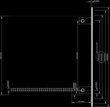
Also here are my dimensions for the PLUS cards I've built (XT-IDE, HardMPU, Memory, and NE2000) so you can cross-check your footprint:
tandy_plus_drawing.jpg

Edit: Just realized the forum decimates the resolution a great deal.

Re-hosted here
 
Or you could use a standard DS12885 with an XO and CR2032 holder and use the 5170 BIOS RTC code to have a driverless clock.

Sure, sounds great, but way beyond my x86 coding ability. Does a version of code to do this already exist in a discrete form to work in an XT? A DS1215 driver sounded like a lot easier problem to handle, I'm reasonably sure I've seen one written in BASIC.

The first post of this thread also makes it sound like it wouldn't necessarily be easier to interface, either, but maybe he was all wrong about that.

Here's a crazy thought... Just put an 22V10 on the first run prototype board in-place of all that speculative logic, work out the solution with a text editor and ROM programmer, and then translate it to discrete 74xx/4xxx logic in run #2.

I'm sorry if my thinking out loud is getting on your nerves. I'm sorry. One glaring problem with that suggestion, alas, is I don't have a 22V10 programmer so I can't just wave my hand and make it happen. First time it came up I did do some digging, and essentially what I found was a bunch no doubt bad information that roughly summarized like so:

1: Circa 2017 the cheapest options were apparently running around $70 on eBay (in 2017), but some of them were really sketchy. To really do it right you need a proper commercial programmer, not some made in China thing that *may* work if you use one very specific device SKU.

2: Found a number of rants going on at further length about how getting a programmer that works reliably is non-trivial.

3: Claims that these chip, while fairly widely available, have been discontinued. Which apparently isn't actually true, probably, but the ones made now have differences...

In short, it seemed like there's a lot of bootstrapping there if you're starting from zero. But I'm sure you know all about this subject and can tell me how wrong I am about that.
 
Also here are my dimensions for the PLUS cards I've built (XT-IDE, HardMPU, Memory, and NE2000) so you can cross-check your footprint:

Since you've built a RAM card for the PLUS slot would you be able to confirm the memory map for add-on RAM starts at 0000h? (or doesn't)
 
If you've got a TL866 programmer, they're "supposed" to be able to program the 20v10 & 22v10 series, though I have no experience with them. Good news is that unlike FPGAs, PLAs are pretty cheap, and Digi-key has the clones available.
How are these programmed? Just write out a truth table in notepad and plop it into the programmer? Or is there a GUI availible?
 
For what little it's worth (obviously I didn't think of it in time) there are some interesting logic simulators out there to let you paint out your problem and test assumptions without burning anything. I just made this:

https://circuitverse.org/users/6802/projects/18960

(you can play with the preview, clicking on the input boxes changes their states) The boxes labeled A16-A19 represent the address line inputs. "CHIP A17" is the output address line routed to the RAM chip, "Enable" is the low-active chip enable output, and D000 and E000 are active low enables for the D and E pages respectively. (Derived from the '138 not included) Walking through the truth table I get this for all 16 possible states of the top four address lines: ("chipadd" is the condition of A18-16 as presented to the RAM chip.)

Page | chipadd | Enable
--------------------------
0 | 010 | 0
1 | 011 | 0
2 | 000 | 0
3 | 001 | 0
4 | 110 | 0
5 | 111 | 0
6 | 100 | 1
7 | 101 | 1
8 | 010 | 1
9 | 011 | 1
A | 000 | 1
B | 000 | 1
C | 110 | 1
D | 101 | 0
E | 100 | 0
F | 101 | 1

Subtract the states where chip enable isn't on and rearrange according to the RAM chip's point of view:

2 | 000 | 0
3 | 001 | 0
0 | 010 | 0
1 | 011 | 0
E | 100 | 0
D | 101 | 0
4 | 110 | 0
5 | 111 | 0

That looks like full utilization of the RAM chip using 4 NANDs ('00), 3 ANDs ('08), and a 74138. But maybe I need coffee.
 
Sure, sounds great, but way beyond my x86 coding ability. Does a version of code to do this already exist in a discrete form to work in an XT?

Of course. Check out: http://retrotronics.org/jride and reference the linked utilities and SVN repo to the left side-bar.

I'm sorry if my thinking out loud is getting on your nerves. I'm sorry. But I'm sure you know all about this subject and can tell me how wrong I am about that.

Just trying to help.

I don't have a 22V10 programmer...

A lot of inexpensive ROM programmers will do SPLDs. Atmel still makes clones as ATF22V10 and are available through most part distributors. It's a good tool to have in your toolbox. I've dead-bugged or proto-boarded several just to simulate a combinatorial logic function in-circuit.

WinCUPL is a horrible program to use. But if you can push through the pain of birth, the baby is worth it.

Since you've built a RAM card for the PLUS slot would you be able to confirm the memory map for add-on RAM starts at 0000h? (or doesn't)

Yes, you map it at zero. I didn't know that until I built one for a 1000A. I've never tried to map UMBs as I didn't have the upper address lines remap'able.

If you prototype it, you can always poke around in debug.exe and see which writes stick.


...there are some interesting logic simulators out there to let you paint out your problem and test assumptions...

Check out a tool called Logic Friday. You can input a truth table and it will optimize row count or generate an equivalent and optimized 74xx series circuit.
 
Of course. Check out: http://retrotronics.org/jride and reference the linked utilities and SVN repo to the left side-bar.

Okay. The chip does still look considerably harder to interface than the smartwatch chip, though. (That only needs a chip select to sit on and like three connections to single address and data lines. This one has a multiplexed data/address bus? Which I'm sure is no big deal with a CPLD sitting in front of it.)

I also already bought the DS1315s and crystals, but if someone else wants to chase this idea...

Just trying to help.

Sorry for being prickly about it. It's just not a suggestion I'm in the position to implement. Not that I think that programmable logic is a bad idea, I just have no grounding in it nor the equipment to do it, so going that route for step #1 throws a *giant* mountain of prerequisites into the way of actually making "a thing".

A lot of inexpensive ROM programmers will do SPLDs. Atmel still makes clones as ATF22V10 and are available through most part distributors. It's a good tool to have in your toolbox. I've dead-bugged or proto-boarded several just to simulate a combinatorial logic function in-circuit.

Do you have any opinions regarding the aforementioned TL866? (Or specifically the TL866II Plus, since that seems to be the current model actually for sale.) The thing that has me worried is I keep finding these threads that essentially boil down to "with (Device X) I could program the (insert brand here) GALs, but ones from (other brand(s)) won't work even though the software claims it was programmed successfully...".

If I could lay hands of a programmer I could be confident in I wouldn't mind learning to use it for some other projects I've had on the back burner for a long time. But I can't justify hundreds of dollars if that's what it takes to get a device that won't randomly screw up in inscrutable ways.

Thank you for once and for all confirming the shape of the T1000's memory map. *Technically* you can derive the right answer from the 1000 EX technical manual but only the original 1000's service manual actually seems to come out and say how it works.
 
I can't speak to most current gen PROM programmers. I used first used a Willem parallel port version when I was a broke college student. 25 years later I have a gaggle of Elnecs and EETOOLS but both are pricey. One could say I'm a bit spoiled.

As for the other design choices.. there is always a version 2! I just found eventually learning a bit of 5V/PTH programmable logic saved a few bodge-wires and re-spins over the years. Good luck. If I had the time to do this sort of thing still, I'd eagerly contribute.
 
Do you have any opinions regarding the aforementioned TL866? (Or specifically the TL866II Plus, since that seems to be the current model actually for sale.) The thing that has me worried is I keep finding these threads that essentially boil down to "with (Device X) I could program the (insert brand here) GALs, but ones from (other brand(s)) won't work even though the software claims it was programmed successfully...".

If I could lay hands of a programmer I could be confident in I wouldn't mind learning to use it for some other projects I've had on the back burner for a long time. But I can't justify hundreds of dollars if that's what it takes to get a device that won't randomly screw up in inscrutable ways.
I've had good experience with the TL866 Plus that I got from Amazon about a year ago. No idea how it will handle older PROMS, but it works with modern CMOS EEPROMS like the Atmel and SSTs that are popular these days, and even has the ability to test logic ICs (which has aided in troubleshooting/repairing one board already).You'll want to look up the compatibility list, of course. The more expensive "professional" programmers will be capable of more, but for the price, it's not too bad for an introductory programmer. The one I got came with extra adapters for non-DIP packages. I've only needed one of those adapters so far, but it gives other options if a through-hole DIP package is impractical for your project.

Thank you for once and for all confirming the shape of the T1000's memory map. *Technically* you can derive the right answer from the 1000 EX technical manual but only the original 1000's service manual actually seems to come out and say how it works.
I'll thank you as well. By the time this is all done, I think we'll both have something we'd be proud to stick in somebody else's machine ;)
 
Back
Top