• Please review our updated Terms and Rules here

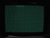
Kaypro 4-83 graphic overlay

Yes I found out timing is crucial and datasheets can be very unclear... I now have replaced both the HC573 latches with 16V8 GAL's as 74F574 are hard to get and I didn't want to wait (...) hoping they might be a bit faster and edge triggered but now I can not even get those GAL's to work properly... Pfff.... They should latch on the rising edge of the clock signal but al I seem to get is 'transparancy'. Need to fiddle a bit more with those.

Also the datasheets of the SRAM chips I have are unclear on what signal the data is stored into the cell, only in the IS61C256 datasheet is an example of using the SRAM with /CE and /OE permanently low and it says the write cycle is then /WE controlled. And then I found out that my GAL16V8's programmed as latches didn't work :)
 
GAL as latch problem solved: seems the compiler refuses to generate registered outputs if either the CLK pin (pin 1) is named, or the /OE pin (pin 11) is named, or you assign output enables to the (registered) outputs. And it does it silently..

Progress so far: if I enable the latch and buffer outputs (and thereby disable the counter outputs) with an additional IO line from the PIO and let the BRDY just handle the /WR pulse for the SRAM it works flawlessy, no more pixel errors. Reading and writing is fine.
Disadvantage of this scenario is speed, I now have to enable the outputs, then perform read or write and then disable the outputs again.
The hash stripes just get longer this way but at least they are black during this period.

The /OE and /CS of the SRAM are now constant at GND level, just the /WR gets pulsed.
 
And another update :)

The stray pixels were generated by address bus conflicts between the counter outputs and the latch outputs.
It seems the 74HC590a releases the output quite slow.

By means of an extra delay in the GAL (connecting an output to an input) I managed to get the outputs of the counters released a little bit before the latches come onto the bus and I can also delay and squeeze the /WR pulse in between. So effectively a write to the SRAM is reduced to a single OUT instruction, that is after setting up the address in the address latches before.
The 'hash' is now reduced to small stripes (about 200 ns in length...)
 
Back
Top