• Please review our updated Terms and Rules here

Mini-Omnibus backplane for debug and minimal system

1. Where are points H2R, H3R, H4R, and H5R? H3L, H4L, and H5L?
sorry, these are points on the +5V distribution trace to the right and left of the mounting holes. Example: H2R is to the left of mounting hole H2, H3L is to the left of mounting hole H3. The hole reference designator is in a very small font on the top side silkscreen. The reason for identifying these locations is that the +5V trace/plane gets narrow near each of the mounting holes, so the corresponding resistance lump in the model is a separate element.

Oh, BTW, sorry again, I forgot to attach the file with voltages that LTSpice computed so you could see the final result.

2. It seems to me that the model needs to also add (at least) 2x 14AWG on the ground return plane when considering the effect of adding the same on the +5v distribution plane. There's not much point in fortifying just half of the +5v power circuit. Considering that the ground return plane is shared with two other power distributions IMO it's the one most subject to "droop" -- which would be in practice "raise" -- at the edge-connectors.
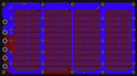
A couple of reasons: the ground plane is almost the entire top side (the red layer in the image) so it's much more robust that the comparatively narrow +5V distribution traces. But with all of the copper clearance around each of the Omnibus connector pins it reduces the effective ground plane width to about 55% of the total height of the board. So, the ground semi-plane (with 1296 holes in it) from the GND power terminal pad on the left all the way to the A2C and A1C connector pads on the right (the right-most Omnibus ground pins) is about 2.2 milli-ohms with 1 oz copper. 12 amps through that is about 26 mV, and then the ground current will actually be distributed to other Omnibus board pins, so the drop will be even less.

Also, the -15V current actually helps reduce the voltage drop through the ground plane because the ground current flows in the opposite direction. So, plug in more core memory and it reduces your ground plane voltage drop! +15V draws 1A max, pretty small. I measured +15V consumption to be about 0.6A on my system, and that's with the KC8E lamps powered from a regulator tied to the +15V.

3. Why not treat (and install) the added wires as a distributed drop in resistance, rather than a single point-attachment?
In the present design the wires attach at specific points: J7 through J10, so the model reflects this. I combined the resistance of the two AWG 14 wires into R8 in the model, since J7 & J8 are close and J9 & J10 are close.

I would strip some 14 or 12 AWG solid wire, form it to the proper "C" shape, and then solder it directly to the copper-plane, ideally continuously but certainly at multiple locations -- the idea being to closely approximate the effect of (distributed) 2oz copper. I've seen this done in various fashions in various other designs, including just being liberal in applying solder to traces to build up some thickness (not as good as pure copper, but it helps). At least I'd add wires dedicated to each of the third and fourth-ranked slot-sets rather than a single (set) added somewhere between them.
It would be possible to lay a thick bare wire along an extended copper area sans solder mask, but there are some issues with that: takes a lot of heat to melt solder over such a large area, adds another labor-intensive step, doesn't look so attractive. And the end result is that the reduction in voltage drop is marginally better only at certain points between what would be the wire ends. Also there are only discrete attach points of +5V to the Omnibus boards, only at pins A2A, B2A, C2A.

Pragmatically I'd focus on building up the "crossbars" that are the terminal distribution legs to the connectors through fully-soldered pieces of heavy copper wire. Particularly the one down-the-middle. Eyeballing (spitballing?) the copper distribution that's where the pinch-point looks to fall given that we're assuming an equally-distributed +5v load across the three connectors of a given module.
This is definitely possible and would probably reduce the +5V drop even more. Ease of assembly, cost and esthetics was pulling me in the other direction. I attached the LTSpice operating point data. Seems good enough, but feedback on that is appreciated.

Thanks for the further enlightenment :-}.
You're welcome.
DC operating point from LTSpice:

Code:
       --- Operating Point ---

V(in_terminal):     5     voltage
V(n001):     4.97899     voltage
V(j7_j8):     4.98654     voltage
V(n005):     4.96903     voltage
V(n006):     4.96812     voltage
V(n007):     4.96477     voltage
V(n008):     4.96386     voltage
V(j6b_port):     4.99324     voltage
V(j9_j10):     4.97907     voltage
V(n002):     4.97718     voltage
V(j9ca2):     4.97286     voltage
V(j8ca2):     4.96971     voltage
V(j7ca2):     4.96709     voltage
V(j6ca2):     4.96501     voltage
V(j5ca2):     4.96347     voltage
V(j4ca2):     4.96248     voltage
V(j3ca2):     4.96201     voltage
V(j2ca2):     4.96209     voltage
V(j1ca2):     4.96271     voltage
V(n009):     4.96369     voltage
V(n010):     4.96303     voltage
V(n011):     4.96285     voltage
V(j9ba2):     4.97488     voltage
V(j8ba2):     4.97256     voltage
V(j7ba2):     4.97049     voltage
V(j6ba2):     4.96866     voltage
V(j5ba2):     4.96708     voltage
V(j4ba2):     4.96574     voltage
V(j3ba2):     4.96465     voltage
V(j2ba2):     4.9638     voltage
V(j1ba2):     4.96321     voltage
V(n012):     4.96218     voltage
V(n013):     4.95981     voltage
V(n014):     4.95914     voltage
V(j9aa2):     4.97136     voltage
V(j8aa2):     4.96733     voltage
V(j7aa2):     4.96398     voltage
V(j6aa2):     4.96129     voltage
V(j5aa2):     4.95926     voltage
V(j4aa2):     4.95791     voltage
V(j3aa2):     4.95722     voltage
V(j2aa2):     4.95719     voltage
V(j1aa2):     4.95783     voltage
V(n003):     4.97346     voltage
V(n004):     4.97336     voltage
I(R75):     -3.10386     device_current
I(R74):     -3.10386     device_current
I(R73):     5.35933     device_current
I(R72):     0.750314     device_current
I(R71):     0.750314     device_current
I(R70):     -0.865324     device_current
I(R69):     0.440696     device_current
I(R68):     -0.424628     device_current
I(R67):     0.440639     device_current
I(R66):     0.0160117     device_current
I(R65):     0.440641     device_current
I(R64):     0.456653     device_current
I(R63):     0.440703     device_current
I(R62):     0.897356     device_current
I(R61):     0.440823     device_current
I(R60):     1.33818     device_current
I(R59):     0.441003     device_current
I(R58):     1.77918     device_current
I(R57):     0.441242     device_current
I(R56):     2.22042     device_current
I(R55):     0.441541     device_current
I(R54):     2.66197     device_current
I(R53):     0.441898     device_current
I(R52):     -0.865324     device_current
I(R51):     -0.865324     device_current
I(R50):     -0.865324     device_current
I(R49):     0.634696     device_current
I(R48):     0.441174     device_current
I(R47):     1.07587     device_current
I(R46):     0.441227     device_current
I(R45):     1.5171     device_current
I(R44):     0.441302     device_current
I(R43):     1.9584     device_current
I(R42):     0.441399     device_current
I(R41):     2.3998     device_current
I(R40):     0.441518     device_current
I(R39):     2.84132     device_current
I(R38):     0.441659     device_current
I(R37):     3.28297     device_current
I(R36):     0.441821     device_current
I(R35):     3.7248     device_current
I(R34):     0.442006     device_current
I(R33):     4.1668     device_current
I(R32):     0.442212     device_current
I(R31):     -0.230628     device_current
I(R30):     -0.230628     device_current
I(R29):     -0.230628     device_current
I(R28):     -0.946055     device_current
I(R27):     0.44113     device_current
I(R26):     -0.504925     device_current
I(R25):     0.441075     device_current
I(R24):     -0.0638501     device_current
I(R23):     0.441068     device_current
I(R22):     0.377218     device_current
I(R21):     0.441109     device_current
I(R20):     0.818327     device_current
I(R19):     0.441198     device_current
I(R18):     1.25952     device_current
I(R17):     0.441334     device_current
I(R16):     1.70086     device_current
I(R15):     0.441519     device_current
I(R14):     2.14238     device_current
I(R13):     0.441752     device_current
I(R12):     2.58413     device_current
I(R11):     0.442032     device_current
I(R10):     -2.27585     device_current
I(R9):     -2.27585     device_current
I(R8):     -8.46319     device_current
I(R2):     11.9157     device_current
I(R1):     11.9157     device_current
I(R7):     -1.17668     device_current
I(R6):     -1.17668     device_current
I(R5):     -1.17668     device_current
I(R4):     1.17668     device_current
I(R3):     -3.45253     device_current
I(V1):     -11.9157     device_current
 
That said, one could compromise by adding IDC connectors to just the _rear_ of the backplane so that the existing 9 slots are preserved for module-use. Those IDC connectors could then either serve as built-in pick-up points for connecting a logic analyzer or use with a modified homebrew version of the M935 Omnibus bridge to extend to a second board to add 8 more slots (and the logic analyzer could then be connected at the rear of the second backplane).
This is an interesting idea, but not without some pain in what it does to the layout. Placing IDC connectors along the back interferes with the +5V and -15V distribution traces. But maybe splitting the +5V jumpers into two and adding jumpers for -15V will solve that. This is adding more assembly steps though. I think most users could benefit from having the IDC connectors considering the combined use of extending to a second backplane or logic analyzer connect points, which I'd find quite useful.
 
Addendum: While I can imagine that your intent here was to model a lumped solution and that in practice you really meant one-wire-on-top-and-another-on-bottom given all of the other specificity in the calculations (! :->)
It's two AWG 14 wires that jumper across a long segment of the +5V trace. The two wires are combined into R8 in the model. Installing the jumpers is quite effective because a pair of AWG 14 wires has about 1/8 the resistance per unit length compared to the 14.5 mm wide trace.
this is an area in which the model is IMO not realistic WRT the calculation of actual voltages (or maybe voltage-differentials) at module-pins ... as opposed to some lumped resistance as seen by the power supply.

But as I noted earlier, I may very well not understand your intent(s) and result(s) here!
I played with moving the loads around to all on a single column of Omnibus connectors instead of being distributed, so all on the "A" connectors or all on "C". The voltage drop was only 20 mV more. The model isn't perfect but accounts for the most significant pieces of copper in the power distribution path.
 
Heck, we might even work a deal where you can help me debug the prototypes.
At the moment I don't have a single operational 8 (E or A in this thread) so I'd be not very helpful :-{. I have been slowly accumulating PDP-8 and PDP-11 equipment/components for almost a decade now, and trying to come up-to-speed while holding down a job (and other commitments). I'm now retired and have hobby-time, but a backlog of infrastructure (and home repairs/enhancements) has been my first priority. Currently I've been working towards PDP-11 topics, but keeping an eye on PDP-8 topics, like this one. Anyway ...

I actually have one of your kits from BITD; it includes a pair of CY62256NLL-70PXC. Uncertain where that leaves me for use with an 8/E, my target environment. Given the liberal availability of prototyping space on that module that's where I'd like to integrate an M837 capability ...
 
I actually have one of your kits from BITD; it includes a pair of CY62256NLL-70PXC. Uncertain where that leaves me for use with an 8/E, my target environment. Given the liberal availability of prototyping space on that module that's where I'd like to integrate an M837 capability ...
The Cypress branded parts work fine, even in the original Lafferty design. There are timing issues with the bus turn-around, which do generate a bunch of transient noise on that card, but it works.

The prototype area is more suited IIRC to DIP designs, and mounting a CPLD would be perhaps a bit clumsy. Lots of point-to-point wiring in either case. Easier and more reliable to replace the PCB, in my opinion. Fortunately, PCBs are still fairly cheap and available, unlike the parts that go into them.

Vince
 
Good to know for my intended use, whew :->. Your target CPLD isn't a PLCC device? What are you using?

I agree that hand wiring/etc. would be a bit clumsy. But standard-size OMNIBUS modules with gold fingers aren't cheap ... AFAIK. 100x100mm PCBs without fingers, now *those* are cheap :->!
 
Thanks for all of the comments! They were quite helpful. v2 review revision 02 has some updates:
1. added a 10th slot.
2. added a 34-pin IDC connector for extending to a 2nd backplane and to connect logic analyzer probes.
3. added a 3rd AWG 14 jumper to reduce voltage drop a little more.

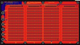
Images of the updated top and bottom layers are here:

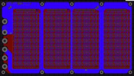
Mini Omnibus Backplane layout top v2 r02.jpg Mini Omnibus Backplane layout bottom v2 r02.jpg

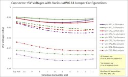
A summary of the voltage drop on +5V at each connector is in the following plot. This is with respect to a single GND common point input terminal. There's a ground plane with many holes in it on the top layer. Taking account of the reduced area due to the holes, the resistance from GND terminal on the left to the ground on pin AC2 in slot 5 on the far right is about 1.9 milli-ohms. If all of the 12A current was focused between those two points there would be a drop of 23 mV in the GND, but distributing the ground current over all of the Omnibus ground pins on multiple slots will result in less voltage drop in the GND connection. GND return current flow from the -15V (being in the opposite direction) will further reduce the drop through the GND plane.

The chart might be helpful to decide whether or not to install the AWG 14 jumpers or to install a subset of jumpers. I recommend installing all three because that' s just the way I am ;-)

backplane v2 r02 voltage drop per connector.jpg

The board will be a bit more flimsy with the added height. Thicker boards cost a lot more, like 2x to 3x. I'll publish a recommended mounting drawing with additional nylon standoffs below the board to provide support when plugging in boards.
 
Am I missing something? How do you use the IDC connectors to connect one backplane to the next? Is the idea to put the connectors on the bottom and run the ribbon cable under the backplane and bring it up to connect in the rear? That would add approximately 7 inches of wire run between the boards right?

I was envisioning IDC connectors on front and rear. This would make about a 2 inch connection between the boards. It would also let you clip your scope or logic analyzer to the front IDC pins for easier access.

I was also looking at the way you snake the -15 between the B1 and C1 pins. Since the trace narrows there could you split it and also run between A1 and B1 to get the width back? The A1 and B1 pins are test points on all connectors. A similar thing could be done on the +15. I've never looked to see how DEC routed the power pins.
 
Good to know for my intended use, whew :->. Your target CPLD isn't a PLCC device? What are you using?

I agree that hand wiring/etc. would be a bit clumsy. But standard-size OMNIBUS modules with gold fingers aren't cheap ... AFAIK. 100x100mm PCBs without fingers, now *those* are cheap :->!
It is an 84 pin PLCC, an ATF1508, assuming they ever come back in stock.

It's been a minute since I last ordered the hard gold fingers, but they used to about double the cost of a board. From the vicinity of $10 per board to about $20, that wasn't bad, if it saved a day of wiring and another day or two of debug.

Vince
 
Images of the updated top and bottom layers are here:

View attachment 1241308 View attachment 1241309

...
The board will be a bit more flimsy with the added height. Thicker boards cost a lot more, like 2x to 3x. I'll publish a recommended mounting drawing with additional nylon standoffs below the board to provide support when plugging in boards.

Thanks George for adding the 10th slot. This will be perfect for all my troubleshooting needs.
The IDC connectors in the back will be very useful for logic analyzer probes and even allow the addition of a second board for those who want more slots.

I would prefer to spend more money and get thicker (more robust) boards made with the thicker copper. The main expense is the connectors and the power supplies not the PCB itself.

I am looking forward to build one of these. Thanks for all your work on this.

Tom
 
How do you use the IDC connectors to connect one backplane to the next? Is the idea to put the connectors on the bottom and run the ribbon cable under the backplane and bring it up to connect in the rear? That would add approximately 7 inches of wire run between the boards right?
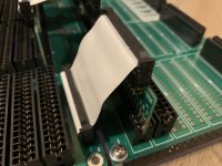
Glad you asked this. I should have described it in more detail. Connecting two backplanes can be done two ways. One possibility is to use one of the bridge boards that plugs into the first slot of the rear backplane and the other end of the flat cable attached to the bridge board plugs into the 34-pin header on the front backplane. The following photo kind of illustrates the concept. This is the version 1 backplane with the Omnibus bridge half-unplugged and I bent the flat cable to show a mock-up of the concept.
connect two backplanes.jpg
The other possibility is to connect the two headers mounted topside by running the flat cable underneath the rear backplane, like this:
Two Backplanes side view.jpg
It does increase the length but the total length is still shorter than a 40-slot PDP-8/E. One possible issue might be with magnetic-field coupling between signals in the cable. There are grounds in the cable but not between every signal. I think this is not likely an issue because the signals are terminated by the Bus Loads board which provides a low impedance load which will attenuate coupled signals. I can test this with my version 1 backplane to confirm the adjacent signal coupling.
I was envisioning IDC connectors on front and rear. This would make about a 2 inch connection between the boards. It would also let you clip your scope or logic analyzer to the front IDC pins for easier access.
That would be nice. I thought about doing this but ultimately didn't. It would be good to get feedback from the group regarding a front header.

Based on recently adding the rear header, I estimate it would increase the short dimension by 9.5mm (about 3/8"). The reason I had some "resistance" to this is there are thick -15V and +5V distribution traces along the front, so they would have to be moved along with all of the copper fill objects and curvy stuff around the mounting holes, so it's not just a simple select-drag-and-drop operation. If this larger size isn't an issue for users who don't cascade backplanes and if the usability is much better for most folks if we have the front header then maybe the front header should be added.
I was also looking at the way you snake the -15 between the B1 and C1 pins. Since the trace narrows there could you split it and also run between A1 and B1 to get the width back? The A1 and B1 pins are test points on all connectors. A similar thing could be done on the +15. I've never looked to see how DEC routed the power pins.
Hey, that's a really good idea! Thanks for taking a close look and for the suggestion.

At first I was thinking we could get by with less thick traces on the -15V, but there's been discussion about plugging core memory into this backplane. I think every improvement to -15V routing is worthwhile. I should probably do a detailed voltage drop analysis of the -15V net assuming there would be a programmer's console, core memory (or two), and bus loads. Does anyone know the steady-state and operating current of the MM8-EJ (8 KW)? The engineering docs I have for the 8/E only provide the currents for the MM8-E (4 KW). Maybe they are similar?
 
George:

Thanks for the additional explanations regarding your power distribution analysis. I'm now "following the bouncing ball". I support the install-all-three plan; important to make sure that those aged tantalum caps pop fast :->!

I don't see the need to go for double-copper, but AFAICS we can simply price that option out when the design is complete and then haggle over the amount of cost-increase.

I'm in favor of a double-thick PCB unless there is very clear guidance (caveat emptor!) regarding adding support at the midpoints (or along the entire length) of the A-B and C-D cross-bars. Ideally those would be screwed in place, but it would be acceptable to simply provide guidance for adding a support of some sort when mounting that would be effective when inserting modules. If we were using DEC-standard SU blocks then the desired support points would also be along the A-B and C-D cross-bars (there would be frame-bars underlying both and the blocks would be fastened down in the middle of each set of 2+4 slots). Lacking standard SU-blocks that make each 2x4 slot section individually rigid we're designing for the use of individual short-depth connectors that will depend completely on the PCB to ensure alignment and resistance to insertion/withdrawal forces. In a bench-top environment that sort of action is intentionally a common occurrence; presumably less so in an 8/E/F/M recreation. Trace fracture/failure is highly undesirable. Other than a double-thick PCB (the S100 folks specify 0.098") I recommend small-diameter attachment points along the A-B and C-D cross-bars - either one in the middle or two suitably spaced along each bar (I recommend two, spaced). Use 6-32 UNC plastic hardware to minimize the effect of the penetration on the trace widths (and I'd add a plastic washer on the top side to spread out the withdrawal stress a bit). Use a non-conductive stiffener along the entire length of both A-B and C-D cross-bars. With the single-thick design IMO it's imperative to add provisions for using 6-32 UNC plastic hardware in two spaced positions along the A-B and C-D cross-bars. Folks are free to use them or not, and back the cross-bars with stiffeners or not. In fact, folks are free to drill your current design for themselves -- which is what I would do. (And add all three wires top-n-bottom, of course :->.)

(I wonder whether DEC-standard SU blocks will fit your design. I suspect not as at a minimum they'd likely require larger drill-holes for the WW posts than you've planned for the connectors.)

I didn't suggest front-and-back IDCs because of the added complexity in the layout plus the additional depth in the two-PCB configuration. If those aren't serious objections for/from anyone then I'm just fine with a 10+2 configuration instead of the current 10+1. +3/8" isn't a problem here; not sure whether +3/4" would be a problem elsewhere. What are the current OD for the PCB?

Have you thought about how your low-profile module alignment/supports might be attached, or is the idea that such would be handled as part of any mounting-environment and then appropriately overhang the backplane on the ends? The power-connection end would require a lot of overhang. Or is the idea to only use such a contrivance on the opposite end of the backplane?

I see an added POK circuit; what's the schematic for that and from where did the design come?

AFAICS your mini edge-to-IDC PCBs are done. Please (eventually ...) post the Gerbers so that we can manufacture some for ourselves. It would be interesting to determine the cost for hard-gold plating on the edge connectors; the PCBs themselves ought to be "dirt cheap". Perhaps Vince has already done this (hard gold plating costing) and it amounts to ~$10 / 4 = ~$2.50 each?

WRT the MM8-EJ (or apparently a comparable MM8-EH), I see that it's a redesign (all three modules are affected), which is what I would expect based on experience with PDP-11 core memory. However the Engineering Drawings seem to indicate that all that was done was to double the number of core planes and add a wee bit of additional circuitry to correspond. I'm more familiar with PDP-11 core memory but I know of no example where doubling the capacity for a module-set didn't result in a complete redesign as typically this was accomplished using a smaller core size and thus somewhat different implementation technology (usually affecting the voltage requirements, not just current). Doubling the power requirements for the MM8-E would be an extremely conservative estimate, although I agree with your intuition that they should approximate that for the MM8-E. A better estimate would be to add perhaps 10% or 20% to the memory-active requirement and the same or less to the standby requirement?

Thank you for all of the additional progress here. IMO you're doing a really professional job of this. When complete I hope that you'll be able to open-source all of the files, including the analysis configuration for the simulation so that others might be able to extend your work to <insert drumroll> A-B-C-D-E-F (hex) ... (yes, I'm thinking about Unibus and others might be thing about Qbus).
 
I don't see the need to go for double-copper, but AFAICS we can simply price that option out when the design is complete and then haggle over the amount of cost-increase.
I agree that 2 oz copper probably isn't necessary, but I can add that option to the voltage drop analysis and people can decide their preferred tradeoff of jumpers vs thicker copper, or both.
I'm in favor of a double-thick PCB unless there is very clear guidance (caveat emptor!) regarding adding support at the midpoints (or along the entire length) of the A-B and C-D cross-bars. Ideally those would be screwed in place, but it would be acceptable to simply provide guidance for adding a support of some sort when mounting that would be effective when inserting modules.
Thought a lot about this and played some with my existing backplane, and agree that something is necessary. In the next post you'll see that I added a bunch of mounting holes that should help a lot. These are at the ends and between A-B and C-D. Thanks for this suggestion! People can choose to fabricate thicker boards, or utilize the additional mounting holes or both.
(I wonder whether DEC-standard SU blocks will fit your design. I suspect not as at a minimum they'd likely require larger drill-holes for the WW posts than you've planned for the connectors.)
I think the DEC blocks that I've seen might have offset pins
I didn't suggest front-and-back IDCs because of the added complexity in the layout plus the additional depth in the two-PCB configuration. If those aren't serious objections for/from anyone then I'm just fine with a 10+2 configuration instead of the current 10+1. +3/8" isn't a problem here; not sure whether +3/4" would be a problem elsewhere. What are the current OD for the PCB?
I tried to add another set of headers to the front but it didn't work out well without growing the board toward the front which is problematic for those who want to use this in a chassis. It would stick out a long ways toward the front. But now I'm taking another look to see if it can be crammed in to the existing space. The +5V power distribution can be affected but I can analyze that and try some test routes to see if it's possible.
Have you thought about how your low-profile module alignment/supports might be attached, or is the idea that such would be handled as part of any mounting-environment and then appropriately overhang the backplane on the ends? The power-connection end would require a lot of overhang. Or is the idea to only use such a contrivance on the opposite end of the backplane?
I'm thinking this is a 3D printed piece that bolts to the mounting holes and has very short card guides that stick upward maybe an inch or two. Maybe providing support on just one side is good enough, but we could also design a piece for the left (power) side.
I see an added POK circuit; what's the schematic for that and from where did the design come?
It's a copy of the Power OK circuit in the H740 power supply (PDP-8/M). It seemed best not to try to invent something new.
AFAICS your mini edge-to-IDC PCBs are done. Please (eventually ...) post the Gerbers so that we can manufacture some for ourselves. It would be interesting to determine the cost for hard-gold plating on the edge connectors; the PCBs themselves ought to be "dirt cheap". Perhaps Vince has already done this (hard gold plating costing) and it amounts to ~$10 / 4 = ~$2.50 each?
Yes, the mini edge-to-IDC boards are done. But I did a stupid thing and saved something else over the top of the design files. However, the good news is that I still have the Gerber files for it so I can publish those. It should be easy to re-create the design files for those who might want them.

These boards are pretty inexpensive, as you suspect. Quoted by JLCPCB with gold fingers (ENIG-RoHS process) they're $22.40 for 10, so $2.24 each. Shipping is extra and varies a lot depending on when you need them. For comparison, without gold, just Lead Free HASL-RoHS - Hot Air Solder Leveling, is $6.20 for 10, so $0.62 each.

Vince's 32KW memory board, with gold fingers, is $32.30 for qty 5.
Not sure if anything is coming out of China these days though. I know JLC tries hard to stay open, but things are a bit different now.
Thank you for all of the additional progress here. IMO you're doing a really professional job of this. When complete I hope that you'll be able to open-source all of the files, including the analysis configuration for the simulation so that others might be able to extend your work to <insert drumroll> A-B-C-D-E-F (hex) ... (yes, I'm thinking about Unibus and others might be thing about Qbus).
Thanks!
I should be able to post most of the files. Some of the analysis files are a bit cryptic and have silly notes for me, but we can try. People can ask if it doesn't make sense.
 
I think the DEC blocks that I've seen might have offset pins
You're correct; the result is a regularly-spaced matrix optimized for wire-wrapping. So no-go on DEC-standard SU blocks, which aren't exactly growing on trees either :-{.
These boards are pretty inexpensive, as you suspect. Quoted by JLCPCB with gold fingers (ENIG-RoHS process) they're $22.40 for 10, so $2.24 each. Shipping is extra and varies a lot depending on when you need them. For comparison, without gold, just Lead Free HASL-RoHS - Hot Air Solder Leveling, is $6.20 for 10, so $0.62 each.

Vince's 32KW memory board, with gold fingers, is $32.30 for qty 5.
Not sure if anything is coming out of China these days though. I know JLC tries hard to stay open, but things are a bit different now.
Note that the "ENIG-RoHS process" isn't hard gold (short explanation: https://www.sharrettsplating.com/blog/hard-gold-enig/); not all PCB processors support hard gold. (One S100-related discussion: https://groups.google.com/g/s100computers/c/toTs4EBHZ8k/m/jZjeIb2XDAAJ; John Monahan has been using PCBCart for this for the past 1K or so PCBs. Very good outcomes!)

WRT Vince's board, I presume that estimate is for the short-board, not the earlier full module-sized board with prototyping area?
 
Note that the "ENIG-RoHS process" isn't hard gold (short explanation: https://www.sharrettsplating.com/blog/hard-gold-enig/); not all PCB processors support hard gold. (One S100-related discussion: https://groups.google.com/g/s100computers/c/toTs4EBHZ8k/m/jZjeIb2XDAAJ;
Sharretts article is interesting, thanks. I'm curious about the concept of "grain surface", will have to research this some more. I think the S100 article is available only to group members.
John Monahan has been using PCBCart for this for the past 1K or so PCBs. Very good outcomes!)
took a quick look at PCBCart. It appears to also be in China. Mini Backplane (lead free process) there is $88 for qty 5, JLC is $27
WRT Vince's board, I presume that estimate is for the short-board, not the earlier full module-sized board with prototyping area?
A larger Omnibus board with ENIG process, such as the M8357R, is $50.60 for qty 5 at JLC. I ordered some in February.
 
I just looked at my 8/e and realized that the Mini backplane won't fit. There is not enough room left to right. The total width of the space for the backplane is 11.25 inches. This includes a gap on the left and right side between the edge of the card and the case of about 3/8". A couple of slots in the back have less room on the right due to the way the cover mounts. The constraint on the right side isn't a problem for the Mini because nothing sticks out on the right and the backplane must be positioned so the front panel is positioned correctly. The problem is on the left side. There is a clearance of only about 3/8" on the left between the edge of the cards and some screw heads that stick out of the side of the power supply. The DEC backplanes are the same width as the cards at 10.44 inches. I think for this to work in an 8/e cabinet the power connections must be moved to the back.

The question is, Will this be enough of a problem to warrant a redesign? This was probably never a design goal so was never considered. I think it will fit in the M case because those are still 19" wide but the power supply is in the back with only the fans on the left to interfere which they don't. The F is either an E or an M, not sure which. Maybe either depending on what was ordered?

This is not something I personally need but I know there are 8/e boxes with only one good backplane.
 
I just looked at my 8/e and realized that the Mini backplane won't fit. There is not enough room left to right. The total width of the space for the backplane is 11.25 inches. This includes a gap on the left and right side between the edge of the card and the case of about 3/8". A couple of slots in the back have less room on the right due to the way the cover mounts. The constraint on the right side isn't a problem for the Mini because nothing sticks out on the right and the backplane must be positioned so the front panel is positioned correctly.
Interesting, I never considered the left side. The updated v2 r03 that you haven't seen yet has been extended on the right by 4 mm (0.1575") so I think the right side will still be okay. It fits in the 8/m which I have. The 8/m has tons of space on the left so I didn't consider it, but haven't seen the inside of an 8/e.
The problem is on the left side. There is a clearance of only about 3/8" on the left between the edge of the cards and some screw heads that stick out of the side of the power supply. The DEC backplanes are the same width as the cards at 10.44 inches. I think for this to work in an 8/e cabinet the power connections must be moved to the back.
Moving to the back might be possible, but I kept the power on the left because I imagined a small mini-box would have space on the left for power supplies and a protection board. This way the power cables would be as short as possible.
The question is, Will this be enough of a problem to warrant a redesign?
Maybe, or maybe there could be a side power version and a back power version. I can explore this a bit and see where it goes.
This was probably never a design goal so was never considered. I think it will fit in the M case because those are still 19" wide but the power supply is in the back with only the fans on the left to interfere which they don't. The F is either an E or an M, not sure which. Maybe either depending on what was ordered?
I have been using my case as a guide along the way, to confirm that the backplane will fit.
This is not something I personally need but I know there are 8/e boxes with only one good backplane.
This is an interesting use case that I never considered, but maybe should if it can be accomplished without too much difficulty.

Oh, BTW, in the version I haven't yet shared, I was able to fit 4 IDC headers in the front. They are *very* close to the first row of connectors so that end of the flat cable will have to be built carefully... it may rub the first connector a little if the flat cable strain relief isn't pulled tight. There's 0.725 mm (0.028") of clearance.
 
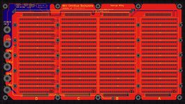
Made some updates based on comments, v2 review revision r03. Thanks everyone for the feedback, it was really helpful!

I somewhat hesitate to post this version while working on the next to attempt to make the board more narrow to fit in an 8/e chassis. Dimensions of this version are:
298.75 mm (11.762") wide by 161.9 mm (6.374") tall. The goal is to reduce the width by 16 mm.

Great comments about the board rigidity and thickness. The design supports this being fabricated on any thickness of circuit board so people can build it how they like. I also added 20 holes for M3 cap screws for those who would like to build it on 1.6mm (0.062”) material and/or have robust mechanical support. I envisioned that the B and C connector rows would be a single edge connector with pins removed and shims installed. There’s now a mounting hole near the end of every connector. It’s of course optional to use these mounting holes. I plan to order 1.6mm boards and use a standoff and M3 screw at each mounting hole, and mount this on an acrylic base.

Changes since v2 r02:
1. Added 4 IDC headers near the front row to simplify cascading two backplanes. The clearance is very tight as mentioned in a the previous post. The Y dimension of the board did not change as a result of adding the headers.
2. Added 20 mounting holes, designators H11 through H30. Pad size supports size M3 cap screws (smaller head so it fits between the connectors). Existing holes H1 through H10 will work with either 6-32 or M3 screws. It’s possible to build with 1.6mm thick boards and use all 30 mounting holes for support, or build with 3.2mm thick boards and use a subset of the mounting holes. It might be necessary to shave the sharp corners of the edge connectors to allow the cap screw heads to fit in between.
3. Board width increased by 4mm on the right to accommodate the 5 holes on the right, H26 through H30.
4. Moved holes H4 and H9 to the right by 0.1mm so all holes between the A and B connectors will be aligned and have the same X coordinate.
5. More robust routing of -15V, added an extra route snaked between pins 1A and 1B as Doug suggested. Also modified the vertical trace on the back side between the C and D connector rows, was +5V, now -15V. This is near holes H11 through H15.
6. Moved the Power OK components to the right in anticipation of making the board 16 mm more narrow from the left side.
7. Various cosmetic changes and minor issues fixed.

Mini Omnibus Backplane layout Top v2 r03 x2.jpg Mini Omnibus Backplane layout Bottom v2 r03 x2.jpg
 
Hi George,
I am very impressed by your willingness to take on all the suggestions which exceed the original design goals and use cases, but make the board more universal.
Thank you very much for doing this work!
Best regards
Tom
 
Thanks, Tom. I’m just pleased that forum members want to built it.

Working on an update, should be ready to share in a day or so.
 
Back
Top