• Please review our updated Terms and Rules here

new to the forum , discovered this existed from the retrobits podcast!

oscilloscope

New Member
Joined
Nov 27, 2021
Messages
5
Location
uk
hi

I'm new to the form , what have i been up too! well in my spare time , i am trying to learn the 6502 assembly of things and other items ! , i have been on a mass buy up of 6502 books assembly language books i have collected devices such as c64 breadbin , and various VIC things. games the list goes on.

my main interest is to learn how to program in assembly. so i have a base of understanding of how chips in general work and what makes then tick! , but i am having great difficulty in reading some of the books i have purchased i would either get stuck on a page and find no real answers which make sense , the book i have started reading again is the "an introduction to microcomputers" , the book is very dated compared to todays computers and hardware. but this is one of the reasons i bought it. , now i did read the first book of this series of books , which again very difficult to read and i realised quite quickly that i know very little about how a computer does what it is , it also doesn't help when i read in general i over think the information and believe it to be harder then it really is it is a very big burden i carry , not to mention my maths skills & English skills are awful.. but fear not i am learning.

so back to the book an introduction to microcomputers"
i have come to page 3-12 to 3-13
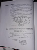
these pages are explaining about " RAM and ROM addressing & memory size & chip select"


i have read this pages alot! its making me dizzy just thinking about it, so the pages start explaining that each RAM chip holds 256(10) memory WORDS , then it leads to another exsplaintions regarding the largest amount of a memory chip which is about 16k i do believe , ( yes this book is old!) , then follows on , with a 2 hex digits of 00 , then follows on about chip select!

right ok , this is where i am getting rather stuck , i have read this over and over and over , so am i correct in thinking this , the arbitrary information , what ever it might be , comes in and is ready to be stored in the ram , but its not stored in say RAM chip one , its spanned across say all 8 ram chips (in the example illustration ) , each piece of stored information has a chip select bit that selects the relevant chip with the correct piece of data. so it knows where it all is?


am i close?
 

Attachments

  • photo64853.jpg
    photo64853.jpg
    154.7 KB · Views: 1
  • photo64854.jpg
    photo64854.jpg
    154.6 KB · Views: 1
Welcome to VCFED.

What is described in the book are examples of memory chips of varying sizes...

The bottom line is that a CPU (such as your 6502) has an 8-bit data bus and a 16-bit address bus - meaning it can (directly) address 1 of up to 65,536 memory addresses - with each address being 8 bits 'wide'.

The address space will be split into multiple separate areas (e.g. ROM and RAM). Some of the RAM may be further subdivided into shared memory for a video screen (for example).

The CPU will start executing instructions from a fixed memory location at power up or reset. It is vitally important that this is in the ROM (for obvious reasons). In the case of the 6502 CPU, the highest memory addresses contain the restart address.

RAM devices come in different 'bit widths' (for example, 1-bit, 4-bits and 8-bits). Whatever chips are used - the result must be an 8-bit wide data bus; so:

8 off 1-bit wide RAMs must be used or...
2 off 4-bit wide RAMs must be used or...
1 off 8-bit wide RAM must be used.

The number of address lines that a RAM chip requires is directly proportional to the 'size' of the RAM chip itself. So if the RAM chip is 256*1 it has 256 internal locations each of 1 bit.

Remember from above that we will require eight ( 8 ) of these in parallel to make up our 8-bit data bus.

In terms of addresses, the RAM chips will require the lowest 8 bits (A7..A0) from the CPU to be fed directly to the pins of the RAM chip to decode the total contents of the RAM chip itself. 8 bits of address = 2^8 = 256 unique internal RAM addresses.

Now, we have to decode the enabling of each 'bank' of RAM chips from the upper address lines ( A15..A8 ) in order to increase the 'size' of our total RAM (as far as the CPU sees it)

You can buy (for example) a 32KBYTE SRAM chip these days and a 32KBYTE EPROM - in this case you would wire address lines A14..A0 from the CPU directly to the RAM and ROM and use address line A15 to decide which devices is enabled. A15=1 means enable the ROM (upper memory) and A15=0 means enable the RAM (lower memory). Of course, the ROM can only be read from (writing to ROM is not sensible and can cause problems). There are usually some control lines from the CPU to tell the address decoding logic when the address bus is actually valid so that data can actually be read and written at the correct time.

Hope this makes more sense than the book - or did I confuse you more?

Don't forget to add your location to your profile if you would like to.

Dave
 
Last edited:
We’re glad to have you here, oscilloscope! It’s great to hear that Earl Evan’s seminal podcast on all things retrocomputing is still bringing folks in. I listened to every episode of the podcast, and got a chance to meet Earl at KansasFest, a number of years ago.

- Alex
 
ok so i have read what you have wrote quite slowly. , so I'm having a information over load right now... some of you're reply has got the me ticking , the fact the 6502 address locations A7-A0 , & the A15 - A1 is going in backwards . which is endianness , little endian. , << hopefully i am correct on that bit!

right so I'm really struggling to understand 8bit part on the page 3-12 , where the 8 separate RAM chips which holds 1 bit in each RAM chip which if i am understanding this 1 WORD equates to 8bits. , and then it has 8 chip select bits? wires? locations ? chip select bits ? abit confusing , and then for some odd reason its saying its a 16bit address when there is only 8 bits of data being stored? , very confusing....then moving across too size of memory address : it has 256 ^10 = 256 separate bits/ WORD's , which would mean according to the example it would need 256 RAM chips to sort the 256 bits or memory WORD's confused ,, further down there is a brief explanation about the largest WORD address , which is 16.384 , then it moves on too the HEX digits.
to say the least i am thoroughly confused.

its taken me best part of an hour to type this to emphasis the confusion , and trying to make it coherent , i'll update my profile
 
ok so i have read the book very slowly. and i keep forgetting that book was written quite some years ago , and the size of the memory is not as big as i assume and it keeps throwing me off the learning curve. and the reason i bought the book is so i can learn about much older computers of things. well go figure aye!

now i am trying to distinguish what a chip select actually means , and how a chip select is used when the 8 bits of data is used up with the data how is a chip select can be used with there is no room to use it.
i kind of get the second page where it explains that if there is a 16bit address but only 14bits is used for the data then the last 2 bits would be used for the chip select. again I'm reading and its not really very clear what that means.

maybe i should sleep on it i have been up since 3am sleepy brain
 
Ah, you are in my time zone!

Anywhere near the M5 (Gloucester) to M6 (Lancaster)? I pass anywhere in between occasionally...

You are still being moderated - so a sensible conversation is not really possible until you get to approximately 10 posts. Just plug away with it for the time being and you will get there...

Forget big/little endian for the time being... That just confuses things. Let's concentrate on the basics.

The 6502 CPU has an 8 bit data bus and a 16 bit address bus. The pins of the IC associated with the data bus are identified as D7, D6, ... , D1 and D0. D7 being the most significant bit and D0 being the least significant bit. The pins of the IC associated with the address bus are identified as A15, A14, ... , A1, A0. Again, A15 is the most significant bit and A0 being the least significant bit.

In order to address memory location 0 (usually referred to in hexadecimal as $0000) all of the 16 address lines are logic '0'. To address other memory locations, the address bus is configured accordingly - so memory address $DEAD (in hex) is [A15..A0] = 1101 1110 1001 1101.

If you are happy with this, we can move on to the next lesson.

Perhaps for the next lesson (as a bit of homework) we will see how the chip selects (not that I have defined this term) work for a very simple 6502 system (see http://retro.hansotten.nl/wp-content/uploads/2020/01/Schematic_TIM6502_V2.pdf.02-scaled.jpg).

Dave
 
Last edited:
There two different things you are mixing up. The 6502 is an 8 bit CPU and therefore needs to work with 8 bit data and instructions. (Software if you will) plus it is a hardware chip that needs external devices (more chips) to store data and instructions. The CPU doesn't care what hardware is used as long as it meets the needs of the CPU. Over the years the older hardware chips have been replaced with newer designs that are either larger in capacity or easier to work with when designing the circuit board. So early memory chips needed 2 or 3 voltage supplies and needed to have refresh cycles to maintain the data stored in them. As cost and chip design improved static ram became larger in capacity and less expensive that the early chips when designing a new board. However, as far as the 6502 CPU when you program it it makes zero difference. All the CPU needs is a boot program in ROM at the correct memory location and storage RAM filling all the other locations. Don't get all wrapped up with hardware talked about in old books that may or may not even be available or would be used on a new design these day.

Some computer designs added external video memory while others shared some of the RAM memory with its programing memory. That was a design compromise either for cost or other other engineering reasons. Again, that has nothing to do with programing except knowing that some memory may have dual purposes due to a designers needs. You will run into this with every old computer you wish to write programs for, not because of the 6502, but due to the designer's limits on cost or board size when designing the computer. Today, a more modern CPU and chips can emulate the Apple, Commodore or other classic 6502 computers and fit onto a board the size of a desk of cards. Software wise it could be designed to act just like the original.
 
Back
Top