• Please review our updated Terms and Rules here

Original-IBM-5150 or IBM-Clone Memory Experimentation Thread

... per the above, it just occurred to me how you could decode 640k with mixed 256k and 64k DRAMs using the same one ‘139.

  • On the first decoder use the outputs corresponding with 0-256k and 256k-512k directly to enable the two 256k banks.
  • Use the output for 512k-768k as enable for the second decoder.
  • Use the lines that correspond to 512k-576k and 576k-640k as enables for the two 64k banks.

Not saying Sanyo did that, but it’s a method that could be achieved with just a few jumpers.
 
I do see quite a few 138 chips. Also, I see jumpers on the board that are either unpopulated or unshorted.

I'll figure it out when I refurbish the board mask.
 
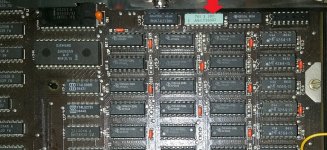
Good news! I've completed the mask repair (The ultraviolet flashlight worked perfectly!) and inserted the memory sockets.

Not so good news, I don't have a display yet, because the memory (512kb at the moment) won't work. (I still have to look at the 5160 schematics to redirect the proper signals.) But for now, my mind is fried, and I can't retain the schematic tracings mentally yet.
 
(This will expand as I look at the schematics)

Ok, on the memory banks, Pin 1 of all the memory chips ( Address Line 8 ) goes to a resistor that is marked "30". (It's on PDF Page 74 / Book Page 1-52 of the 5160 Technical Reference) I'm a bit confused because I don't know if that means just ohms or kilo-ohms.

EDIT: Never Mind, the resistor is indeed 30 ohms. (I measured it with a multimeter)

Update: It does indeed seem that Sanyo had intended to make the MBC-775 or (maybe) similar models expandable to 640k. Address Line 8 is attached to the 30 ohm resistor, which is tied to pin 4 of the additional LS158 chip, just like on the 5160 schematic. I'll check the rest of the circuit upwind from that, then see where the buffer delay line needs to go. (I detached that because the factory patch wire leading from the buffer delay line to the LS158 seems to be in a different place on the schematic, and I needed to detach it to clean the final through-hole and insert the chip socket for the LS158.)

Update 2: Ok, the 158-to-buffer-delay-line wire should stay where it was. (It's ok, I've been taking pictures before I change anything, to prevent problems in reversing small mistakes)

On the other hand, it's odd, because the delay line IC in my Sanyo does not match the schematic exactly. It's actually supposed to be on Pin 3 (IBM) instead of Pin 4 (Sanyo), but the pin for that delay (60ns) is not present:

IBM's Pins (TTLDL-20):
12: 20ns
4: 40ns
3: 60ns
6: 80ns
5: 100ns

Sanyo's Pins ( 201JHT1006L, assuming equal divisions, because the datasheet does not have delay markings, and this was the only datasheet I could find!):
11: 25ns
4: 50ns
10: 75ns
5: 100ns

EDIT: I'm also assuming that the memory bank CLOSEST to the CPU is bank 0? (I'm checking if I have the memory ICs in the correct sockets.)
 
Last edited:
Ok, I've run into a small problem. The A/B inputs of the extra 158 are not connected to any of the Y outputs of any 244 chip.

According to the schematic, they should be tied to a 244 chip that is grounded. I don't know what ICs they are on my Sanyo yet, but it's easy to figure out. On the IBM, though, they are U14 and U16

EDIT: Ok, it seems they are all grounded on the Sanyo.
 
Last edited:
... per the above, it just occurred to me how you could decode 640k with mixed 256k and 64k DRAMs using the same one ‘139.

You were talking about this? Guess what I happened to find over near the buffer delay line IC? A footprint for an LS139. That may be what I need.
 
Right now, and for the past day or so, I've been mapping out the connections between the LS158s and the LS244s. (based on the schematics in the 5160 Technical Reference)

Some of the pins on the 158s don't go anywhere. I'm wondering if I can use a free LS244 input-pair to tie the memory in properly...
 
At first glance, the memory decoding seems to be controlled by four 224 chips, and two 373 chips. (Along with the 158s and 138s)

(Again, this is at first glance. I'm not saying that there are more yet.)
 
Ok, there's three 158 chips, two 138s, four 244s (yeah, I called them 224s by accident), THREE 373s, and three 245s.

The thing with this setup is, the way they are wired does not match the schematics of the 5160. Probing the pins of the chips and checking continuity doesn't show the same pathways as the schematics. (I can post my findings later, if you want.)
 
Here's what I've found so far, based on my continuity checks:

The resistors that are on Address line 8 for the 256k (64kilobyte) chips are where they should be and at proper values. (They're in the schematic with the 158s below) The buffer delay line is where it should be.

However, the chips and their setup in decoding the contents of memory seems different, somehow.
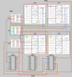
Here's my routing of the pins between the chips (I may have gotten some wrong, because as I routed them, some don't make sense):
Sanyo Pin Routingflat.jpg


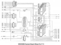
And the IBM 5160's first stage of the memory-decoding circuitry (158s):
MEM.jpg


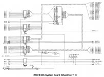
And its second stage (244s and 373s):
DECODING.jpg
 
Last edited:
At first glance, the memory decoding seems to be controlled by four 224 chips, and two 373 chips. (Along with the 158s and 138s)

I had a longer reply to this typed up, but then I accidentally trashed it because backspace is evil, so here's a shorter version: it feels like you're a little confused what a '244 and '373 do. Neither of these things are "controllers". A '244 is just a unidirectional buffer/line driver; whether it's asserting what it sees on the input or goes into an invisible "tri-state" condition can be switched on and off, but that's it, it doesn't care at all about the contents of the data/address lines piped through it. (Note also that control lines like MEMR/MEMW/whatever are also commonly piped through '244s because a '244 is often employed to increase the TTL "fan out" of a signal that's tapped by many consumers.) A '373 is likewise just a latch; based on the status of a control signal it either transparently rebroadcasts on its output what it sees on its input, or it "freeze-frame"'s it and holds an instantaneous state on the output until the latch signal is released. (The reason the 373's are there is because of the multiplexed bus of the 8088; the same pins are used for addresses and data/status signals at different parts of bus cycle.)

The "decoder", IE, the thing that decided what bank of memory is active when address "X" appears on the buffered/latched address lines in the 5160 is chip U44, which is a programmed 24S10 1024x4 bit PROM. It's pretty literally a "black box"; its inputs are A16-A19 (which means it has 64k granularity), the state of a couple DIP switches saying whether a given pair of sockets is enabled at all, and some jumpers which I *think* say whether a given pair of banks has 64k or 256k chips in it, and what comes out are some signals that say which of bank 1 through 4 (or none) are turned on. (This part of the schematic is pretty confusing because the four outputs from the PROM are gated in several odd ways and go to both the "Q" inputs and the output enables of the RAS/CAS '138s.) If the Sanyo has a similar PROM, or possibly another programmable device like an early PAL, in this position then your best option is probably to find a compatible part and program it how you need.

If there is no PROM on the Sanyo board then you need to figure out if they *did* actually make full allowances on the board for the 640k option. This is where putting the manual for the 64k/256k 5150 alongside the 5160's manual will probably be instructive. Compare the memory decoding circuitry and *basically* the difference is instead of the RAS/CAS '138s being directly linked to A16 and A17 (also note they get an input from another '138, U48 who's *actually* ultimately the thing that says RAM should be active in the lowest 256k of space by sitting on A18 and A19) they are "abstracted" through that PROM. IBM didn't have to do it this way; to expand the 5150's decoding to support 256k on a pair of the sockets they could have, for instance, used additional outputs on '138 as inputs to U47 and U65. (I'd need to sit down with a piece of paper to work this out, but I think you could reshuffle it to work, possibly with the addition of a couple of NAND gates.)

Long story short, I think you need to bite the bullet and actually draw out the schematic of how the Sanyo derives the CAS/RAS signals for each memory bank. If it doesn't use a PROM like the 5160, which there's a good chance it doesn't, you'll need the complete layout of how it is *now* to figure out how to hack it properly.
 
Last edited:
No, I understand that the chips are not controllers.
I read the datasheets for them. I understand that these chips do some kind of data-scrambling logic and channel-switching "magic" to turn the information in memory into something the CPU understands.

I'm just contemplating if tying the A16 and A17 data lines into a free spot in the logic circuitry will make it work, like changing how a floppy drive interprets grounded setting pins. (This is tentative, though. I know it might not be as simple as that.) The other data lines seem to be added already.

Update: Right now, I'm setting up a new pin map to see if I can find a pattern in how the logic lines are connected.
 
Last edited:
No, I understand that the chips are not controllers.
I read the datasheets for them. I understand that these chips do some kind of data-scrambling and channel-switching "magic" to turn the information in memory into something the CPU understands.

They don't "scramble" anything. The '244 is literally just a valve. (Or maybe "two valves" because it has a separate control "handle" for each 4 bits of the total 8 bits it handles.) The inputs, usually designated "1A(1-4)" and "2A(1-4)" on the datasheets, are controlled by the signals "1G" and "2G" respectively. If the "G" for those four bits is low the input state (high or low) is presented on "1Y(1-4)" or "2Y(1-4)" respectively; if "G" is high the outputs assume a "high impedance" state which essentially renders the device invisible. (Which means a downstream device either gets high or low from another device, a pull up/pull down resistor, or just floats.) When you see a '244 in a circuit the "G"s are often tied to ground, which means it's basically just acting like an "amplifier" for the input signal. If it *is* controlled it's usually because there's something else connected to the output side and the 244' is acting as part of a multiplexer.

(For instance, a pair of '244s could be used to do roughly the same job as a pair of 74LS157 Quad 2-input multiplexers, IE, either could be used to decide if the 8 bits to be asserted on "Bus Z" were sourced from "source X" or "source Y". The control circuitry would just be slightly different.)

A '373 does the same thing (IE, it can act as a "valve" because it has an output enable signal to tri-state the output, although in its case it applies to all 8 outputs simultaneously, not two groups of four) except it can also "latch" what's coming out the other side. IE, if output enable is "low" then what comes out on the "O" outputs matches the "D" inputs in real time if latch is "high", but if latch goes "low" the value on D0-7 is latched into into registers "Q0-7", and that value is what comes out on "O0-7" for as long as latch is held low, regardless of what happens to "D0-7". Again, nothing gets "scrambled"

I'm just contemplating if tying the A16 and A17 data lines into a free spot in the logic circuitry will make it work, like changing how a floppy drive interprets grounded setting pins. (This is tentative, though. I know it might not be as simple as that.) The other data lines seem to be added already.

No. A16 and A17 are not "data lines", they're address lines, and they're no doubt already "connected to the logic circuitry" that's used to select which set of RAS/CAS lines are active because decoding A16 and A17 is how you tell which page of 64k you're on. (IE, like this: 64K takes 16 bits to represent; IE, if the smallest chips the Sanyo supports are 64K we can completely ignore A0-15. That leaves A16-A19. That's 4 bits, which allows 16 possibilities, which means a total of 16 possible pages of 64k to think about. When you only have 4 banks and they all have 64k then this is what your decoding needs to care about to decode your RAM, which should reside in the bottom 256k of the possible 1024k of address space:

A19 - Has to be a zero
A18 - Has to be a zero

(This is what U48 does on the 256k 5150 board does. If A19 and or A18 are not a zero then the '138s that decide what bank is selected don't do anything.)

A17 and A16: Again referencing the 5150 schematics, these are decoded by U47 and U65. These are set up to act as 1-in-4 decoders (see how half the outputs are "wasted"; looking at the IBM schematics it looks like IBM used them instead of '139s because they're relying on the multi-conditional output enable gates to add additional conditions beyond the address to gate the assertion of these signals) and which set of CAS/RAS signals is active, IE, which bank is enabled, is *directly based* on the state of A17 and A16. There's nothing more to do with them.

To make your Sanyo access 256k in a bank you actually need to disconnect A16 and A17 directly from the CAS/RAS decoders (assuming that's how they're actually wired, that's why I said you need to figure out if there's a PROM, additional decoding, or *what* there) and instead generate a truth table something like this:

(x = "don't care".)

Code:
A19 A18 A17 A16 : Desired state
 0     0     x     x   : Enable RAS/CAS for bank 1 (256k, starting address 00000h)
 0     1     x     x   : Enable RAS/CAS for bank 2 (256k, starting address 40000h)
 1     0     0     0   : Enable RAS/CAS for bank 3 (64k, starting address 80000h)
 1     0     0     1   : Enable RAS/CAS for bank 4 (64k, starting address 90000h)
 All other states      : Nothing enabled.

Note also that the first layer of decoding, U48 on the 5150, which is "active low" when *any* of the banks should be active, was also used as a control signal for several items, including a bidirectional '245 buffer in front of the RAM data lines, so whatever you do on the Sanyo to fix the RAS/CAS decoding also still needs to produce that total "memory is active, period" signal. So, again, it's A18 and A19 that you need to start decoding in more detail to get more than 256k, and that is where it matters critically how the Sanyo is doing it *now*.
 
Thank you. I'm sorry if I don't sound like I'm up to the task.
There's a lot of jargon to sift through too, and I don't always get them right (despite my knowledge) and things lately haven't exactly been spring chicken.
I do understand that there are lines that go from the CPU to memory. (Maybe not directly. Again, though, I tend to get them mixed up.)

However, I've seen videos about how memory (Doom's cheat codes), and read about how disk contents [Apple II Disk II writing-to-disk methods], can be obfuscated, so I assumed that there was some shuffling/scrambling of groups of bits here and there to re-create the proper data grouping for the CPU to understand.

The tracing of the pathways makes a bit more sense now.

G, on [Sanyo] U45 and U47 is indeed attached to ground.

Right now I'm reworking my pathway tracing to make it easier to read and organize. I'll see if I can look a bit more into the logic of the chips.
 
Last edited:
This mapping is already getting complex, but I'd like to see what I can do.

I have noticed patterns that are cropping up:

The 158s are all at least connected to an input (on one chip) AND an output (on another), forming a complex series of logic valves.
Control pins (that control the impedence / basic on-off state) are all connected to GND.


The good thing is that the RAS and CAS are indeed connected to 138s. Now I just need to figure out where those 138s figure into the picture.
 
Last edited:
A bit of progress today. I got my 64-kilobit chips in today, and I now have a full 640k of memory, which matches the amount in the 5160 schematics.
I'm still mapping out connections, but it's slow because emotionally, I'm spent because of this quarantine.

I'm betting that the logic connections don't match exactly with the IBM schematics; maybe what is the difference is that the connections are logically the same (same type of input pins, same type of output pins), but connected to different pin numbers because of routing differences in manufacturing?
CuriousMarc did the same thing when performing repairs on a Xerox Alto. One logic gate within an IC was bad, so what he did was rerouted those signals to an unused gate of the same type on the other side of the chip, which allowed them to temporarily make progress until they could source a new modern-built version of the chip.
 
A bit of an update: looking at the schematics, this Sanyo is looking more and more like a 5160 clone. The components are all matching up in number and type to the schematics so far. I just need to find out what components are not connected properly.
 
Been a while. I got some UV EPROMS and burned a copy of the Supersoft Diagnostics. The diagnostic gets stuck at the 8253 Timer 1 check.

I get One Hi-Lo and 8 beeps. It suggests the 16k critical memory area is not working.
(Unless I'm misinterpreting, and the Hi-Lo means two beeps, in which case it says the numeric co-processor isn't working, but it seemed to work when I used the Landmark Diags about a month or two ago)
 
Last edited:
Ok, further investigation shows that the memory refresh is not occurring, due to Timer 1 not operating. I'll check it tomorrow and see if there's a wire that needs to be connected to the memory from there.
 
Back
Top