• Please review our updated Terms and Rules here

Pet 3016 (upgraded to 32k) just getting $FF from RAM in diagnostics

Bagpuss

Member
Joined
May 14, 2023
Messages
30
Location
United Kingdom
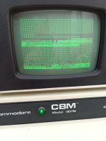
Hi, ina. Bit of a dilemma with my PET
I burned the diagnostic edit ROM from Daver2.
I replaced the static ram as they were bad. I replaced the CPU with a good working one as I suspected that.
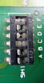
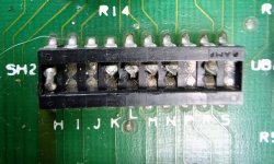
I've pulled the 3 I/O chips to be safe and eliminate them interfering.
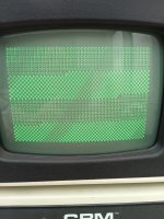
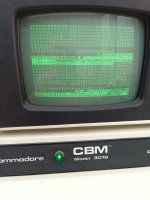
So far on the diagnostics of zero page it's giving me $FF for all reads. I replaced the 74LS244 buffers closes to the dram and tested the lower 3 4116 to make sure they were good (not done the whole lot but at least checked a sample set).

Given that the screen is good I expect E9 and E10 are good. If I pull the 244s buffers near the dram it continues to give $FF. Those chips test OK in my tester as well.

I was thinking next, is the dram refresh circuit bad causing the dram to loose values, but that doesn't seem to be the case (or at least as far as my oscilloscope skills get me, I can see RAS0 toggling).

I'm kind of at a loss now on where to go next. DRAM and buffers test good. Address decoding should be right else the ROMs wouldn't work. I can see CAS0 strobing so address decoding to zero page must be at least reasonably OK.
Refresh seems to be doing something.

Crystal gives 16MhZ,, 1MHz clock is good, sync must be working as the ROM diag runs, interrupt is high, clocks on CPU are good, else it wouldn't run. Just seems the DRAM circuit will only ever return $FF.

I'm thinking next use a logic analyser and pulse values into output pins of selective 4116 chips.

I've ordered a romulator from bitfixer but not hear anything yet and shipping to UK is a job in its own right these days.
 
There could be something wrong in the logic controlling the DRAM reads and it is returning FF's.

Since page 0 DRAM defects prevent the computer from booting (I assume that is what is happening ? ) and the lower 1k is important for BASIC to work normally, I devised a way to dynamically deactivate DRAM reads in the lower 1 or 2k of DRAM and switch in support SRAM to allow the computer to boot and then perform diagnostic tests on the DRAM, helpful in cases where they are soldered in. It is explained in this article:

www.worldphaco.com/uploads/DRAM%20MEMORY%20TEST%20SYSTEM%20FOR%20THE%20DYNAMIC%20PET%20COMPUTER.pdf

In there are over 20 scope recordings of the DRAM support circuitry, which remains active even if the computer is doing nothing. You could use those recordings as a reference.

Did everything check out with the NOP generator before you moved to Daver2's PETTESTER ?

There is also the trick, suggested for DRAM diagnostics, to switch the /CAS1 and /CAS0 lines to switch the upper and lower DRAM banks. Generally done by lifting one end of the series resistors and crossing them over.
 
Last edited:
As this is your first post, welcome to VCFED.

Also, thank you for using my diagnostic tool...

Can I suggest updating your profile to include your location? I guess you are also in the UK from your post?

You will be under moderation for your first 10 posts, so things may go a little slowly to being with...

My first question is - how do you know that the DRAM is returning $FF?

Can you post a photograph of the video screen (just to convince myself)?

/RAS0 will be togging for two (2) separate reasons - a DRAM refresh and a DRAM access from PETTESTER. You have to differentiate between the two before you can state that the refresh circuitry is working.

Dave
 
Hi , thanks. I've not got a Nop tester (laser ran out of stock but have new ones coming in :) )

I've been following Desperado's thread too, followed all the testing steps there on page 38, I get pulsing as expected on Ras, cas0, g1 pins, I replaced g7 just because I thought it odd that cas1 was not pulsing (I assume that it would pulse to do dram refresh) but after that it's still sending cas1 high so assume that's because it's not accessing it.
I was wondering if the upper 4116 ram was having an issue and sending the data bus high, testing the latter 3 of the J row they all check out fine as well as the first 3 chips of I row.

H4 looks OK from signals WE low is happening and all the pin 14 pulses etc behave.

One thing I'm wondering about is the circuit around the 16mhz crystal as it didn't look as clean as I would have liked but that could also be me needing to dial in my oscilloscope probes.

My logic probe is happy at 50MHz so has been able to detect pulses. My oscilloscope is an old hammeg analogue one so it's not quite as easy to see traces on it's CRT that a digital affair.

I've been going through the schematics with coloured felt tip pens marking up all the paths through the pages and writing down on each pinnwhat should be there, e.g. high, low, fast pulse, slow pulse, so far it's all behaving.

Also last night double checked all my ROM/CPU pins for continuity.

I may go the heck of it stick the 6502 from a BBC model B in there (I probably can't go the other way as the Beeb is clocked at 2Mhz)
 
Welcome to the forums.
Thanks. First battle is the PET, next is the twin floppies.
So far I have resurrected an Apple II, 4 apply floppy drives and a very sorry state bbc master :)
The pet is something that my son really loved the look of, so when I saw an old 3016 I had to get it :)
 
As this is your first post, welcome to VCFED.

Also, thank you for using my diagnostic tool...

Can I suggest updating your profile to include your location? I guess you are also in the UK from your post?

You will be under moderation for your first 10 posts, so things may go a little slowly to being with...

My first question is - how do you know that the DRAM is returning $FF?

Can you post a photograph of the video screen (just to convince myself)?

/RAS0 will be togging for two (2) separate reasons - a DRAM refresh and a DRAM access from PETTESTER. You have to differentiate between the two before you can state that the refresh circuitry is working.

Dave
Thanks. Image attached. The marker for it being $FF is that the final byte of zero page and page one tests as good which coincides with PETTESTER ticking up by 1 as it writes each byte. The faulty results on screen match the petscii symbol for $FF. It behaves the same if I pull the 4116 RAM as well so I assume that RAM floats high by the time it hits the 6502 data lines.
That they are lower case g's and b's implies to me that the sram is good.
As PETTESTER runs I assume the main address decoding is fine as as cas0 toggles then address line BA14 is behaving.

Forgot to add, in terms to ras0, both pins 13 and 14 are toggling on G1 to generate pulses on pin 11. I think I am.makign an assumption that H3 driven by G5 is generating refresh.
I'm still rather new to the internals of a PET so I'm not sure if I'm making wild assumptions and stabbing in the dark :)
 

Attachments

  • IMG_20230516_181512_427.jpg
    IMG_20230516_181512_427.jpg
    4.3 MB · Views: 7
Last edited:
>>> I thought it odd that cas1 was not pulsing (I assume that it would pulse to do dram refresh)

DRAM devices refresh on the RAS cycle not the CAS. The PETTESTER is only testing out the first 2 pages of RAM (512 bytes) as this is a critical area for the 6502 CPU. This lives in the first bank of 16K of DRAM - so this explains why only /CAS0 is operating and /CAS1 is not.

>>> One thing I'm wondering about is the circuit around the 16mhz crystal as it didn't look as clean as I would have liked but that could also be me needing to dial in my oscilloscope probes.

The high frequency signals on a PET are horrible at the best of times!

>>> I've been going through the schematics with coloured felt tip pens marking up all the paths through the pages and writing down on each pin what should be there, e.g. high, low, fast pulse, slow pulse, so far it's all behaving.

Good man! Excellent process skills...

Dave
 
>>> Image attached. The marker for it being $FF is that the final byte of zero page and page one tests as good which coincides with PETTESTER ticking up by 1 as it writes each byte.

Very good - you read the manual! That is a first here :)!

Dave
 
Thanks. I had a read through the source code to see what it was doing, hence that it must be presenting $FF.
Now the tricky bit to analyse is if it's trying to write $FF then reading OK, read is always getting $FF or just ignoring what is coming from RAM.
 
Can we just double check the two link blocks in your machine by posting a photograph of them?

Dave
Hi. Here you go. The history of this was that it was a 16K machine, the upgraded to 32K. It looks like all the link blocks are set up as I would expect (I hope).
 

Attachments

  • IMG_20230516_201317_642.jpg
    IMG_20230516_201317_642.jpg
    519.8 KB · Views: 4
  • IMG_20230516_201328_056.jpg
    IMG_20230516_201328_056.jpg
    974.7 KB · Views: 4
I had a follow on though. I think the refresh looks oOK on the surface, so the next possibility if that is correct is that at least 1 dram out of rows I can J for each but is faulty, possibly when going open circuit getting interpreted by the 244 buffers as high. I think that would tally up with pulling the dram 244 buffers still resulting in $FF.
I think in that case, If I remove a couple of bits from both I and J, and perhaps pull pin 14 low (not sure what resistor value to use here) then I should see two bits in the test go low and the screen pattern change.
If the pattern does not change then I think that says the issue is between the 244 buffers and the CPU or the address decoding is going wrong.
 
You can prevent the DRAM from responding by disconnecting the /CASn lines from the driving ligic and resistors and pulling them up to +5V with a 1k resistor.

You can then use a 1k resistor to pull the data lines of the DRAM low in sequence and observe the results on the screen.

EDIT: It would appear simpler to use a wire link and pull G7 pin 1 to 0V. This should disable the two G7 gates driving /CAS0 and /CAS1 and force these signals permanently HIGH. It is OK to pull a TTL output signal (H4/12 in this case) LOW.

This simple trick should prevent you from requiring to remove any DRAM chips.

Dave
 
Last edited:
Have a look at the scope recording on page 11 of the article I posted. If the DRAM IC is non-responsive for any reason, the voltage on its output pin can be interpreted by the buffer as high or low, depending on the timing. One would guess it would always be logic high, but it is not always. So if you deactivate the DRAM by disconnecting the /CASn lines and tying them high, and you want to apply a specific bit pattern on the DRAM outputs for testing, likely the effect will be the same and it is better to put either a pull up or a pull down resistor on the outputs to create a bit pattern.

I found it odd that Commodore didn't use a pull up resistor array, because in diagnostic testing at least, homing in on defective IC's, this effect can cause variability in the returned byte values. There are examples of this effect in the article with non-responsive IC's. The effect though is ok, if you are ready for it and know that it can happen.

One way would be to wire in all 10k pullups and use 1k for the pull-downs as Daver2 says.

Though if you are just looking for a change in the bit pattern and not a specific byte, then it is probably not necessary.
Thanks it was a good read, particularly around the high/low issue.

I tried swapping out the high 3 4116's from both row I and J which didn't make a difference.
Next job will be to pull them low. My though are if that doesn't work then it's probably address decoding at fault.

Thankfully my Nop generator turned up today which I was well impressed with as laser said they had new stock on the way yesterday morning :) so I'm going to read through how to use that in the desparado thread as well.

Though possibly not tonight as it's Elite Dangerous night with my friends from US :)
 
So big-ish step forward.
Ran through all address lines with the Nop adaptor installed. Addresses cycled fine.
The started tracing down the road and CAS lines. Whe. I got to pim13 of G1 the pulse was fine coming out of H1 pin 6, but on entering G1 at pin 14 it was stuck high. This did not make sense to me. My assumption was that H1 is asserting the pulse but there is enough garbage going on at G1 pin 13 to generate a high ( would have expected H1 and G1 to be the same).
G1,H1 and F1 looked like they had corroded pins so I replaced them all with new chips.
It's made a difference, I started getting cycles of garbage returned. Left it for 10 mins to do a video and it returned back to the normal $FF.
So tomorrow is probing time again :)
 
Actually after some probing and checking signals I get some rotating garbage on test as per screen shots as an example.
It looks like zero page is fairly static but the upper 512 bytes cycle. What I see on H1 pin 16 looks like it's going from 2.5v to 5v rather than 0 to 5 in a pulse (I need to check it again in case it's an oscilloscope issue) and when the signal hits G1 pin 13 it looks like it's degraded as if has a curved transition to high, but is going from 0v (this may mean I need to swap out my other probe). I'm going to check and see if any soldering has created a slight short tomorrow though as well.

Update: H1 logic gate 3 failed test on my logic tester.
 

Attachments

  • IMG_20230517_195000_863.jpg
    IMG_20230517_195000_863.jpg
    4.2 MB · Views: 6
  • IMG_20230517_194959_795.jpg
    IMG_20230517_194959_795.jpg
    4.3 MB · Views: 6
Last edited:
Can you post the schematic you are using. The IC references don't appear to to match my dynamic PET schematic. And Pin 16 for most 16 pin IC's is the +5V rail.

H1 in my PET is a 74S74 which is a 14 pin IC (most people don't stock the "S" series and have to order them too, unless they have a very extensive TTL collection) so your H1 cannot be the same part as mine.

If a pulse goes from 2.5V to 5V it suggests either the output transistor in the gate has become defective, or something is pulling it up with a much higher than usual current. This is the sort of level you can get with two tri-state devices fighting each other too on a bus with some contention. One way to find out if an IC pin is overloaded, without damage is to just solder suck that output pin and free it in the hole. And you can then also test its current sinking capability by adding a pullup resistor, to confirm if the output pin is normal, or not. A TTL output should be able to pull down to a solid low with a 330R pull up resistor.

Generally speaking with connections between TTL's, if a level is wrong, it is the output stage that is defective, less likely the input stages they drive in other IC's. While the inputs can go open, not uncommonly, they seldom source too much current. Though there was a very oddball case on a PET board a while back where two inputs in a gate shorted together inside an IC, which then rendered two outputs driving those fighting each other at times, but it was the only case of that I have ever seen working with TTL's since the 1970's, and I have my doubts about it, as it could have been caused by a solder bridge or tin whisker that got destroyed when the IC got replaced.
 
Last edited:
Back
Top