• Please review our updated Terms and Rules here

Pet 3016 (upgraded to 32k) just getting $FF from RAM in diagnostics

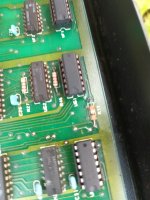
Sorry my typo it's pin6. I put in a 74ls74 under the assumption that is was compatible with a 74s74 (i.e. it's the lower power version).
I'm going to get bmy desoldering gun out tomorrow and remove the sockets and check for shorts. I suspect I have a possible bridge under the socket.
 
The S might be compatible, but it might not. Sometimes the higher power parts are chosen because they are faster and have shorter propagation delays and in some circuits it could cause a pulse's leading edge to arrive later with a slower part, with respect to some other pulse elsewhere and cause a malfunction. So it is hard to know if it would be an issue or not. A plain 74 type is closer to an S than the LS is. But it is "probably" ok, but it does make you wonder why the designers used the S, they must have had a reason and likely it was a timing thing, rather than a drive fan out thing, because it only connects to a few gates.
 
Last edited:
Hi, I think post end of day I was having a typo session. As G1 pins are 11 12 and 13 for the logic gate. I'll do another probe. I wanted to get a photo of the oscilloscope but I need a third hand for that :)


Looking at the datasheet for the s74 Vs ls74, the pulse turn is 6ns Vs 20ns so it may be they are selected due to a faster switching time. I've seen in the schematics both LS and S used so it may be specific variants.

I've ordered a batch of the locally as they are quite cheap.
 
Last edited:
As a follow up. I was being a dumbass.
I didn't even notice that one of the 244 buffers had lifted itself out the socket with me rotating the board etc. So reseated that and I'm back to the usual $FF screen.
Following the traces, I can see the not Q (H1 pin 6) making a nice pair of pulses, thrnse should be reaching p13 of the G1 nor gate but they don't. With the crappy one from yesterday I'd say it's a trace or bad solder issue. So that is tonight's job. Trace h6 to g13 and if necessary replace the socket I put in G1.
 
At some point in time we have all done dumbass things!

It is only people that don't do anything that never have those sorts of moments...

Good hunting.

Dave
 
And to quote an old Sepultura song " Under a pale grey sky he shall arise"

The pet is past the rams screen.

Fault were -
one of the H1 flip flops was bad replaced
The signal going from h1 pin 6 was good. Receiving at G1 pin 13 as random between a bad saw tooth wave and just low on different tests. Traced though from h1 pin 6 across the motherboard to work out the path. Traced to first via, good. From first via to second via (about 8 to 10 mm) got no signal.
Did a little scrape across the trace, was good from via one to.kidway align the trace but not good the other way.
Replaced the solder on each via, no joy. Visual inspection it looked OK so I decided to solder a wire wrap wire between via one and via two.
Bingpot ! I got passed the zero page test.
The via even has a flipping "1" next to it as if saying "test this first" :)

It's now passed two cycles of ram tests as well. Time to verify the check sums for basic 4 and burn the edit ROM back to to the eeprom.
 

Attachments

  • 16844319993823012493880437605429.jpg
    16844319993823012493880437605429.jpg
    3.4 MB · Views: 6
Last edited:
Well done!

I would give the DRAM a good 20 (Hex) passes to be sure though.

This test really thrashes the DRAM...

Dave
 
Thanks. I'll take a couple of days off as I have to brace myself for the floppy drive. That at least looks like a zero page ram fault.
 
Don't forget to test out the IEEE488 port first. There is a test BASIC program available that will test this out.

Yep, check that the ROM checksums are stable and that the keyboard works using PETTESTER.

There are a few threads around on repairing the disk drives, but you need a known working PET port first!

Dave
 
There must be a track fracture between those two vias. It may well be worth looking at that again with high magnification to try to find out what caused that, corrosion or something physically striking the pcb or whatever, just in case whatever the cause was, it could be affecting other nearby tracks in the future.

(One trick to disconnect a track for the purpose of modifications to a pcb, if there are vias, is to run a small drill through the via, just big enough to remove the copper in there, then latter if required a small wire link can be placed in there to re-establish the connection to undo it, it is a better method than cutting a pcb track with a knife)
 
Thanks. I forgot to say as well. The basic 4 eeprom I have varies by one byte from the normal one. On a brief look at it I think it may be a patch rather than faulty. I'd check my dump tonight and see if I can disassemble around the difference.
 
It's ud7. It checksums to A42d instead of A425
Byte at $0809 is $06 instead of $00
Looking at the binary I think this is jmp $BF08 instead of jump $BF00 based on the disassembly . Bf00 is the syntax error routine. Bf08 would be jumping into the not function.
The routine at D804 is used by Scratch and header and jumps to syntax error if the accumulator is not $E6 (which looks like a result of checking file parameters on a disk command)

It's quite possibly that it's just one bit stuck in the eprom.
 
Is it an original PET ROM or is it a Uveprom or a eeprom that someone programmed as a replacement for the original part ?
On one of my PET boards, two of the original ROMs were defective, but it was pretty global with many bytes damaged, not just one byte.
 
Hi it's a uveprom. It's odd they just own byte is damaged and it looks like only a jump when handling a syntax error. Perhaps it was burnt wrong and never noticed
 
Back
Top