daver2
10k Member
Ok. That sounds perfect.
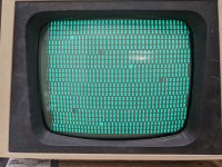
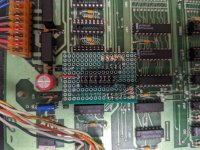
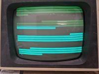
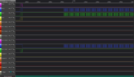
For each logic HIGH you should get one complete vertical line of pixels in each column of characters. The image on the screen should be completely stable.
If you pull-down all of the data line outputs, you should have a completely black screen.
If you pull-up all of the data line outputs, you should have a completely white screen.
The more pull-ups you have, the more vertical lines of illuminated pixels you should have.
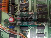
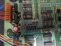
If you notice in your first picture, you have some slight differences over the screen image.
Dave
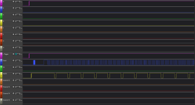
For each logic HIGH you should get one complete vertical line of pixels in each column of characters. The image on the screen should be completely stable.
If you pull-down all of the data line outputs, you should have a completely black screen.
If you pull-up all of the data line outputs, you should have a completely white screen.
The more pull-ups you have, the more vertical lines of illuminated pixels you should have.
If you notice in your first picture, you have some slight differences over the screen image.
Dave