• Please review our updated Terms and Rules here

PET reset switch circuit with a condensator for pulling the diagnostics line down

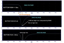
For momentary press ( less than ~1 seconds, /RESET and /DIAG go low and high in unison. So by the time the CPU has started looking for the /DIAG line, it is high and a normal RESET is performed.

View attachment 1258315

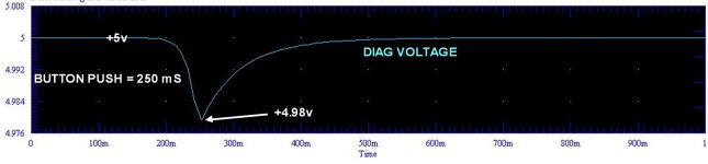
For a longer press, /DIAG is held low, and /RESET slowly ramps up to HIGH ( about 3.8v, though may be more or less depending ) over a matter of seconds. Once /RESET reached logic HI, the RESET operation starts while the button is still pressed and /DIAG is LOW.

View attachment 1258316

When the button is released, both go high, but as /RESET is already HI and /DIAG has been read, so it won't matter. This design does not require a bi-level switch, and only GND, /DIAG and /RESET. This should work if reset action actually occurs from a LOW --> HIGH transition. You can probabaly futz around with the value of the capacitor and resistor. "At least in the simulator" LOL It also assumes /RESET is the CPU's reset line which halts on logic low, and performs the reset transitioning back to HIGH.


That circuit won't work properly in the actual PET for two reasons:

One is there is no resistor to discharge the capacitor and turn the circuit to its original state prior to the next use of it (except for extremely low diode leakage). So it will only work once for a reset and that function will fail after its first use once the capacitor is charged. Also when the computer is line powered of, after that, re-powering it will take the side of the capacitor connected to the diode to -5V. Its easy enough in the simulator to set the capacitors initial voltage at 0, but you have to consider how it could get back to that state later.

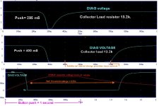
On my PET at least, the minimum resistance value on the DIAG line to pull it low enough, that it is interpreted as a logic low is close to 3.3k, for example a 4.7k won't do it, so modelling the source resistance for that at 100k won't work. This is one of the many reasons I used a transistor to drive the DIAG line, so it can sink enough current to get a solid logic low.
 
Further to the DIAG line issue as noted (in my PET at least) the minimum resistance to ground on the DIAG line to be interpreted as logic low is about 3.3k. With this resistor in place experimentally, the voltage across the 3.3k resistor is close to 1 volt. Very similar in fact the the voltage required on the /RESET line to be interpreted as logic low, it is less than one volt. It is acting as though the internal pullup resistor in the PIA is roughly about 13.2k Maybe that varies with the brand of PIA IC, not sure.

I have attached some of the simulator recordings of my circuit with the transistor. One other beneficial feature of the transistor (whether the original unit used one or not, we don't know for sure) is that because of the knee of the B-E junction of voltage vs current, the transition of the DIAG voltage from a definite logic high to a definite logic low is only about 60mS so the period of a "logically ambiguous voltage level" is relatively short compared to the slow charging profile of the capacitor. And any voltage on the DIAG line > than about 1V is interpreted as logic high. Actually the ambiguity shrinks to a some 10's of millivolts on either side of the 1V threshold where the DIAG pin is interpreted as high or low.
 

Attachments

  • DIAGA.jpg
    DIAGA.jpg
    272.9 KB · Views: 5
  • DIAG4.jpg
    DIAG4.jpg
    72.7 KB · Views: 5
Last edited:
I took a few more recordings from the simulator. The simulations above were using a 1K resistor for the transistor load, if I altered that to 13.2k for the attached simulations, to better represent what the DIAG line in the PET behaves as (my PET at least), the switching point is a little more sensitive with a slight left shift in the graphs.

Plotting the DIAG voltage with the capacitor's charge for a long push such as 1 second, shows that the capacitor's voltage levels out to 0.95V (as expected) at about 600mS and after that, after the button is released from a long push, the DIAG stays low for a while as the capacitor discharges into its discharge resistor and the transistor's B-E junction too.

The circuit also demonstrates something else, which I knew about from using a transistor's B-E junction as a voltage reference in a switching application. The Silicon signal transistor's B-E junction starts to conduct at around 0.50v and by 0.6v it is conducting significantly, with 0.55v to 0.56v being the figure where the transistor's collector-emitter circuit represents about 10k and this is the actual central threshold voltage for a signal transistor as a switch, especially if its collector load resistance is in the order of 10k. When a silicon signal transistor is in a switch-mode supply application, and its B-E used as a voltage reference with a switching signal, the average base-emitter voltage (integrated measurement) usually measures around 0.55V. This is the way it is in the car Alternator voltage regulators as one example. It is good that the simulator agrees.

To check this, if you set up a transistor like a BC338 in a simulator, grounded emitter, with a 5V Collector supply and a 10k collector load resistor, and put a voltage source in its base, with a series resistance of anywhere from 1 Ohm to a few hundred ohms, you will find that the collector voltage will sit at about 2.5V when the base voltage is about 562mV. (of course in real life that arrangement is temperature unstable due to the -2.1mV/degC temperature coefficient of the B-E junction). In the Alternator regulator though, they cleverly cancel this temp coefficient out by using a series 7.5 to 9V zener diode in series with the base which has a positive temperature coefficient. Lucas built a transistor with the zener diode inside it.

The graphs of course are easily shifted to the right, just by increasing the 4700uF capacitor value.
 

Attachments

  • DIAGF.jpg
    DIAGF.jpg
    277.4 KB · Views: 6
If you look at the PIA line used for the /DIAG signal, it is also an output (it drives the sounder).

It starts off as an input and then becomes an output (in my mental model anyway).
I don't think that's right. (Sorry for jumping in in an old thread, but since I have been quoted via the PETdoc document upthread I feel somewhat involved :)

The Diagnostic Sense line (pin 5 on the user port) connects to PIA 1's PA7 pin, one of the 2 8-bit ports. Sound is created with CB2 from the VIA (pin M on the user port). At least according to the schematics in http://www.zimmers.net/anonftp/pub/cbm/schematics/computers/pet/2001 and thereabouts.

The way this line has an effect on the boot process is that the kernel, pretty early in the reset sequence, checks for it, and if pulled down, jumps to the monitor instead of going on to Basic. In particular it does this before the destructive memory test, which makes it so useful to recover from crashed programs. After that initial check, it is no longer used.
I think it's supposed to be used with one of those hardware diagnostic harnesses that plug into various ports.
 
Last edited:
Ahead of the sounder is a 74LS00 NAND gate with one input connected to the /DIAG pin and PA7 of the PIA.

If the input is HIGH, sound will be produced (assuming the VIA is producing it).

If the input is LOW, sound will not be produced.

It is just possible that pulling /DIAG manually LOW causes any BEEP to be disabled of course and that the PIA PA7 is always configured as an input.

I would have to check the EDIT ROM sources to see how the PIA was initialised and managed.

As you say, it is a while ago now...

Dave
 
I was perusing the BASIC 4 disassembly this afternoon.

The PIA containing Port A with the /DIAG bit appears to be initialised as four (4) inputs (PA7..PA4) and four (4) outputs (PA3..PA0).

The outputs are used to drive the keyboard signals.

It would appear as though PA7 is configured as an INPUT - with the "passive" pull-up resistor being on Port A of the PIA.

With the signal pulled-up (via the PIA passive resistor) this sets the one input of the NAND gate (driving the sounder) HIGH - so the PET can produce the chime on demand from the firmware.

Part of the PET EDIT I/O initialisation code generates the chime.

After the PET EDIT I/O initialisation has taken place - the KERNAL code (starting at address FD3E) checks to see if PA7 is pulled LOW. If so, the diagnostic monitor will be entered in preference to BASIC.

An interesting observation:

If PA7 (/DIAG) is pulled LOW at any time - the PET sounder will be disabled (via the NAND gate).

By this mechanism, if /DIAG is pulled LOW when the PET is turned on / reset then the sounder will not chime.

Dave
 
Ahead of the sounder is a 74LS00 NAND gate with one input connected to the /DIAG pin and PA7 of the PIA.
Ah now I remember something. Actually I first noticed this in the emulation code in MAME, and then too I was thinking "what the heck is going on there?".

It turns out that this NAND gate and /DIAG is a new thing, added in the models which do have the piezo speaker thingie. If you look at the schematics that I looked at (the 2001N ones), then it isn't there.

I think (I don't remember if I read this somewhere, or came up with it myself) it was added as a compatibility thing. PETs were seemingly often used because of their many digital outputs, and if somebody used a PET's CB2 output for some process control purpose, then replacing the PET board with a newer model would suddenly have an annoying sound output.

On the other hand, this seems like a weak argument: it requires a software change (program the DIAG line as output and pull it down). Also it loses a potentially used I/O line. A hardware change in the form of simply destroying the speaker is much simpler.

On the pro side, it kind of fits with the apparent strategy that newer board revisions seem to have various jumpers for disabling new stuff.

I think the usefulness of this NAND gate is so low, that I'm not emulating it in VICE.
 
Back
Top