Ya, I guess I will start with your ending of the message.I checked among other pins 35 and 36 por in case I made a mistake and was a 8203 instead. However, to work accordingly with the memories it has and to work with an external clock both pins should have been tied to +5V, which is not the case. I am sure it is what I said... On the other hand could it be that the controller in the slave card was a 8203 configured to work in 16k mode? How could I have some kind of confirmation on that?
I found a direct connection from the 74LS670 on the edge of the board to the ROS memories. If two registers were for the CPU memory map and the other two were for DMA use, It would only amount to 128KB per bank as the registers are only four bits. Something is missing from my scheme, it's just I still don't know what it is.
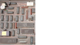
By the way, your boards look gorgeous. I am glad they did survive... My unit only has the floppy drive controller board so it will be difficult for me to ever come close to one of those.
I knew they released it late because they wanted BASIC compatibility with the S/34, but other than that I ignore what is the degree they implemented. Please, have in mind I started with this system a year ago and work on it had been halted most of the time - my experience is very limited. I wish I knew half the things you know - that's why I am asking.")
Don't worry about your experience is very limited and that the system was parked for a while.
As you are probably aware and some others are also aware that most of the technical information on the system 23 no longer exist any ware online. (Schematics and register information).
So this information has to be rediscovered you could say. That takes some time to do of course. Now I will try to give you some suggestions to the 128K memory issue.
..
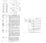
Hopefully I don't get to many typeo's in this reply - It has been quite a while since I did anything with the 8202 and 8203 DRAM Ctrls, but I have done a couple of quick pages hopefully this helps.
As a reminder, remember that their are jumper on the mother board that control how much memory is installed in the system 23 memory card slots. (This information is in the technical manuals
located at bitsavers,org archive for the system 23 computer). For those who want to know more about it.
..
As for the Intel 8203 and 8202 issues with the 75LS670 only seeing 128K per bank, what is likely missing is the upper bank register selection lines and yes, the memory controller in the slave card a 8203 can
be configured to work in 16k mode, there was older logic board version that had used the 8202. On some models of the System 23 below the 500 models only so much memory is available through the memory
card slots and the rest of the systems address space is only available to the expansion card slots. (The additional address lines are not wired to a jumper location for the DRAM Controller to be able to access them).
A lot of early IBM mainframe and minicomputer systems have 2 memory registers one for Address to 16M range and another one for addresses over the 16M range, And yes on some IBM Mainframes only half
of each register is used the rest are reserved.
..
The Intel 8202 supported up to 128K Bytes without external driver circuits added. The 8203 in 16K mode Pin 35 is tide to VCC or is left open then two blank select inputs are active.
In this mode the 8302 is backwards compatible with the Intel 8302 DRAM CTRL. In 64K mode pin 35 on the 8203 is tied Gnd, this lets one bank select input pin 26 be active for 128K.
..
A lot of early IBM systems have 2 memory registers one for Address to 16M range and another one for addresses over the 16M range, And yes on some IBM Mainframes and minicomputers only half of each register
is used the rest are reserved. As a small hint, on most Intel 8085 based Multibus boards that only supported 128K of memory without a MMU intel had a jumper to connect the 8085's SIO signal to the Address line
A16 directly.
..
The bug thing is on the clones you can separate Stack space into two pages of 64K each, one for Stack data and the other for Stack Control data, plus the fact that you can separate the memory further into Program
Space and System Space, that both have there own 64K space for Data or instructions. This is normally done with external logics when using a Intel 8085 or Zilog Z80 microprocessor.
..
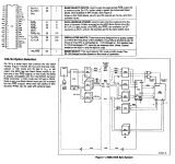
For more Information on using the Intel 8202 and 8203 DRAm Controllers is :
To find Intel's designers notes for the 8202 and 8203 DRAM CTRLS or a schematic for a 3RD parity memory expansion unit for the Sinclair QL that used the 8202 or 8203 DRAM Controllers that allowed
for 256K to 1M byte of extra memory. To use 8K or 32K dram chips they are pulling a couple of the AH and AL signal lines hi depending on the DRAM Chip being used. To use 128K DRAM chips they redirect the
bank select inputs to a higher address line and are disabling half of the memory's A8 signal line. (Some times called RAS2 on some DRAM Chips), depending on the DRAM Controller.
..
Luckily I had some free time today to reply to your inquiry.
Remember that their are jumper on the mother board that control how much memory is installed in the system memory card slots
Attachments
Last edited: