• Please review our updated Terms and Rules here

TRS-80 Model 1 RS-232

Ugh.

Was holding off on pressing the 'submit' for the PCB Gerber files pending one more revision. I pinned the 40-pin IDC header for the Model 1's expansion bus connector, but annoyingly Tandy did not number the pins to convention - they inverted the numbering on the rows.

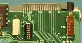
On the TRS-80 PCB, pins 2, 4, 6, 8..... 40 are on the top while pins 1, 3, 5, 7....39 are on the bottom. Argh. I am going to have to invert pin pairs (1, 2 to 2, 1 and 3, 4 to 4, 3 etc) on the pin-out of 40-pin header and re-wire.
1656591127786.png
 
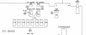
Annoyingly, this is a widely published diagram of the expansion port pin-out, allegedly as "viewed from the rear of the keyboard assembly":

1656599919788.png

I fixed this diagram by rotating it 180 degrees!

When viewed from the rear with the keyboard facing the correct way up, pin 40 is on the top left and pin 2 is on the top right.
"Sam's Computer Facts" at least gets this right:

1656600092872.png

As I don't own an original Model 1, I am using this PCB photo with the pin numbering on the silkscreen to be my definitive reference:

1656600228148.png
 
Annoyingly, this is a widely published diagram of the expansion port pin-out, allegedly as "viewed from the rear of the keyboard assembly":
The CPU board is installed in the keyboard case upside down. So I believe all of the diagrams you referenced are correct (without flipping)...
Doesn't mean you don't need to flip the connector on your board, but it sounds like it you do it would have to install on a "real" Model 1 upside down?

BTW - I haven't checked in for quite a while, but I followed your original build closely and it's nice to see you're still giving it some love. (y)
 
The CPU board is installed in the keyboard case upside down. So I believe all of the diagrams you referenced are correct (without flipping)...

Yes, I was going to point out the same thing. In an original Model I the motherboard is attached to the upper case, component side down, so both the photo and SAMS book show it in that upside down position.
 
The CPU board is installed in the keyboard case upside down. So I believe all of the diagrams you referenced are correct (without flipping)...
Doesn't mean you don't need to flip the connector on your board, but it sounds like it you do it would have to install on a "real" Model 1 upside down?

BTW - I haven't checked in for quite a while, but I followed your original build closely and it's nice to see you're still giving it some love. (y)

Hey, good to see that you are still around. :)

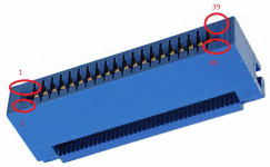
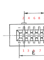
Doh - now that explains why the odd numbered pins appeared to be on the bottom of the port, but Tandy still ran the number order in reverse to convention (hence my confusion). See the image below of an IDC edge connector. The pin numbers are mounded into the case and can be made out fairly easily. If you plug one of these into a TRS-80 the correct way up, connector pin 39 will mate with PCB pin 1 and connector pin 40 will mate with PCB pin 2.

This means that the IDC pin header on my PCB needs to be rotated 180 degrees and I still need to reverse the pin pairs as rotating the header swaps around the odds and evens.

1656611194232.png

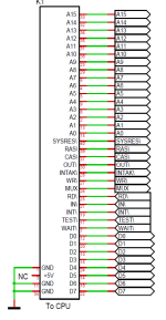
In another thread I started someone posted a reverse-engineered schematic of the Expansion Unit buffered cable. The wiring of the IDC PCB header shows what needs to be done (note that there is a error in this schematic which swaps the +5V with a GND pin, but +5V was modded to GND on Level II Model 1's anyway).

1656612225658.png
 
Doh - now that explains why the odd numbered pins appeared to be on the bottom of the port, but Tandy still ran the number order in reverse to convention (hence my confusion). See the image below of an IDC edge connector. The pin numbers are mounded into the case and can be made out fairly easily. If you plug one of these into a TRS-80 the correct way up, connector pin 39 will mate with PCB pin 1 and connector pin 40 will mate with PCB pin 2.
Or did convention not take the precedent set by Tandy into account??? ;)

I do seem to recall getting bit by IDC pin numbering quite often (back in "the day"). I suspect one could dig up examples of just about every possible pin numbering scheme if they were so inclined. Super bummer that this didn't become obvious before actually ordering the PCBs...

Too much flipping for me to visualize right now - but have you considered whether you might be able to install the connector on "back" side of the board to address the flip? (probably not, but thought I'd throw it out there).
 
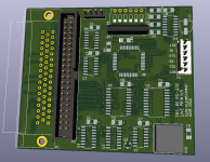
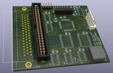
Hah. Fortunately I still haven't hit the submit button on my cart, so the PCB isn't being made yet :) Both flipping the pin pairs and rotating the whole header 180 degrees was the easiest way to wire the header as per the buffered interface cable schematic shown above, with minimal and easy rerouting of my existing PCB. I've actually completed this now, but I am left with a PCB with a ribbon cable entry in the opposite direction to what I originally intended:

1656619567813.png

When plugged into an original Model 1 with an IDC cable, the board will have to be orientated so that the RS-232 header (P4) faces the expansion port. This is less than ideal and a bit annoying. I can of course fix this by rotating the header 180 degrees back to its original orientation, but that is then a major re-route to keep the current wiring.

Argh. Currently mulling over my options and cursing Tandy for numbering the pins in reverse.
 
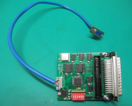
So after much testing I am just about ready to sign off on V 1.0 of the firmware. Aside from writing this project up, it is basically done now.

I've programmed this device with four different selectable serial modes and 8 baud rates.

DIP switch positions 1, 2 and 3 set the baud rate from 1200 baud to 115200 baud.

DIP switch positions 5 and 6 select the mode. The modes are:

0. Basic line printer. Send only.
1. Receive only
2. Receive only with hardware flow control
3. Basic Terminal. Send and receive

Mode 0 is for BASIC Line Printer commands LPRINT and LLIST. This mode is intended for "printing" to a terminal program capable of capturing the output. DIP switch position 4 turns on/off the auto-insertion of LF after CR. This function only applies to Mode 0. Mode 0 doesn't require any driver software. Data bit 7 of port 0x37E8 on the read side is the BUSY bit. This bit is used by the UART firmware for flow-control when inserting a LF. Alternatively, any data value POKE'd or other wise written to port 0x37E8 when in this mode will be transmitted by the UART.

Mode 1 allows the TRS-80 to receive 8-bit data bytes over RS-232. A system interrupt is used to signal to the TRS-80 that a received data byte ready to be read at port 0x37E8. Individual data bytes must not be sent at intervals quicker than what the TRS-80 can read them in from port 0x37E8.

Mode 2 is Mode 1 with the addition of hardware flow control. This is controlled by the UART's RTS output which connects to the CTS input of the sender. Hardware flow control is more efficient than inserting delays between sent characters at high baud rates. In this mode, after the TRS-80 has read in a received byte at 0x37E8, it has to signal to the UART that it is ready to receive the next byte by writing any data value back to 0x37E8. This data value is not read and is not sent. The write strobe is simply used to signal the UART to request the next character from the sender.
With RTS/CTS flow control enabled in your PC terminal program, whole files can be transferred to the TRS-80 in this mode at any of the selectable baud rates.

Mode 3 is a very basic terminal communications mode without flow control. It emulates mode 1 on the receive side and prioritises data reception over transmission. Any attempt to send a byte by writing to port 0x37E8 will be ignored if the UART is busy receiving incoming data. On the transmit side, this mode is not compatible with the line printer commands LPRINT and LLIST. This is because port 0x37E8, on the read side, is now fully utilised for the transfer of received data and cannot faux line printer status.
Mode 3 doesn't require any driver software on the write side. Any data value POKE'd or otherwise written to port 0x37E8 will be spat out of the UART at the selected baud rate, provided that the UART isn't busy copying incoming characters as already mentioned.


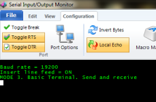
The device configures itself as per the DIP switch settings immediately after power-on and reports the configuration status at the selected baud rate:
1657777811384.png

The UART master reset input is connected to the TRS-80's !SYSRES line, so pressing the NMI reset button on the TRS-80 will cause the UART to reconfigure itself to any change made to the DIP switch settings.
 
Last edited:
Are you planning on doing a run of these to sell? Or publishing the files open source?

I have a L2 Model 1 and am happy with it being a cassette system but not having real IO is kinda a bummer. I don't want to deal with getting a whole clunky EI just for rs232.
 
I plan to publish the design files on my site. I've just been sidetracked with other things and busy in a new job and haven't progressed much with the projects documentation since my last post. Give me a few more weeks. I'll post here again with a link when it's done. I am otherwise no longer interested in participating in anything forum related anywhere.
 
I plan to publish the design files on my site. I've just been sidetracked with other things and busy in a new job and haven't progressed much with the projects documentation since my last post. Give me a few more weeks. I'll post here again with a link when it's done. I am otherwise no longer interested in participating in anything forum related anywhere.
Ok thank you for sharing your work. I will check back in a few weeks.
 
Back
Top