• Please review our updated Terms and Rules here

Vector Graphic ZCB /PHANTOM + Power-on-Jump Error

glitch

Veteran Member
Joined
Feb 1, 2010
Messages
5,051
Location
Central VA
I've been using one of my Vector Graphic ZCBs in my test board set for a while, and ran into a bit of trouble with it tonight. I'm wire-wrapping a static RAM board that, among other things, supports /PHANTOM. It seems that, if you have the ZCB configured for no Power-on-Jump, /PHANTOM is still asserted until something in the ZCB's memory range (0xE000 - 0xEFFF, 0xFF00 - 0xFFFF with default jumpering) is accessed.

This seems like incorrect behavior (it locked out my RAM board since I'm not using a monitor ROM on the ZCB), plus completely unnecessary. It looks like the rev 2 ZCB disables the DATA IN bus drivers if it's accessing anything onboard (ROM, RAM, serial, parallel) so it wouldn't need /PHANTOM for POJ anyway. The board doesn't assert /PHANTOM normally for onboard device reads unless you specifically jumper it.

Thoughts? Someone want to look over the ZCB schematic and double-check my findings?
 
glitch said:
.../PHANTOM is still asserted......Someone want to...double-check my findings?...

Probably Revision 1:
http://maben.homeip.net/static/S100/vector/brochure/Vector ZCB Brochure.pdf
States: "PHANTOM - Output buffer disable compatible with Vector Graphics PROM/RAM boards, which generate phantom in response to Power-on-clear (POC). Jumper selectable: On/Off. Standard: enabled."

http://maben.homeip.net/static/S100/vector/cards/Vector ZCB Single Board Computer 198006 Rev1.pdf
Sheet 4 of 9, shows jumper "C" as the enable/disable site.

2.3.6 Phantom enable/disable
. . .Jumper area C
. . .Connections as manufactured: jumpered.
Function:
. . .Allows generation of phantom on S-1OO bus line 67. When enabled,
. . .phantom disables other system memory cards. This is useful when
. . .you want to jump to a particular EPROM on system power on/reset.
Options:
. . .to disable the generation of the phantom signal cut jumper between
. . .both pads of jumper area C.
 
Last edited:
took a look at the schematics tonight [rev.2],
is this the version you have ?
​​​
On Mon, Sep 8, 2014 at 12:01 AM, Systems Glitch systems.glitch@gmail.com wrote:​


(also posted to vintage-computer.com forums)

I've been using one of my Vector Graphic ZCBs in my test board set for a while, and ran into a bit of trouble with it tonight. I'm wire-wrapping a static RAM board that, among other things, supports /PHANTOM.

​what was the addr range of that new Ram card again ?


It seems that, if you have the ZCB configured for no Power-on-Jump, /PHANTOM is still asserted until something in the ZCB's memory range (0xE000 - 0xEFFF, 0xFF00 - 0xFFFF with default jumpering) is accessed.

I see on sht.4 that /PHANTOM with the Jumper C option still IN, will allow this to be asserted always during any memory access to onboard Rom & Ram. And it does get asserted at POC or RESET via the FF at U27.


This seems like incorrect behavior (it locked out my RAM board since I'm not using a monitor ROM on the ZCB), plus completely unnecessary. It looks like the rev 2 ZCB disables the DATA IN bus drivers if it's accessing anything onboard (ROM, RAM, serial, parallel) so it wouldn't need /PHANTOM for POJ anyway. The board doesn't assert /PHANTOM normally for onboard device reads unless you specifically jumper it.


​This does look like incorrect behavior and this indicates it is not S-100 compatible. But then S-100 had several derivatives back then, so what is compatible, until the ieee-696 boards came out.

VG apparently​ ​assumed you would *only* use their configuration in the system. Because /PHANTOM is only supposed to be asserted during a qualified memory access and not arbitrarily at /Reset [or /POC]. Plus the fact that /PHANTOM is allowed to be asserted by any card, not only the CPU card.

But in this case, the VG ZCB is hard wired to assert this signal alone -- not a preferable method. This is supposed to be clarified in the S-100 docs. But I noticed that there were several cards which did not implement this properly. As a result some mods were needed when building a system using boards from several different vendors [or making your own]

​​
On Mon, Sep 8, 2014 at 9:30 AM, Systems Glitch systems.glitch@gmail.com wrote:​

On Mon, Sep 8, 2014 at 5:50 AM, Dan Roganti ragooman@gmail.com wrote:​

​>
> I see they are both Enabled by default - Jumpers are IN.
> You mentioned that you disabled POJ jumper,
> it didn't sound like you disabled the Phantom jumper

Correct, /PHANTOM can be used to block out arbitrary chunks of address space even if it's not in use by an onboard device, so I want to be able to keep using that feature.

> I supposed that the addr decode is still activated and asserting Phantom
> even though you disable the POJ jumper, which is probably just a CS signal

It looks like POJ /PHANTOM is asserted when the board's power-on clear RC circuit goes low at startup, and the flip-flop isn't reset until something in the onboard device block(s) is accessed.


You would have to modify that section on sht.4 to operate better. Basically, if you want to remove the POJ jumper option at B, then have an associated Jumper option to disconnect the Preset on the FF at U27. with an added pullup on the preset pin so it doesn't float and inadvertently change the state of the FF when the jumper option is removed.

This will prevent the ZPU from always asserting the /PHANTOM at /RESET. But at the same time it will still assert /PHANTOM during any qualified memory access to onboard memory via U13 or U5.
​Dan
 
​noticed something strange last night, but had to crash after that, I wanted to look at it again when I woke up

That Phantom circuit continues to look more strange each time I look at it.
From what I see, that signal never gets released after a memory access to onboard memory.​
The only signal that toggles the /phantom signal is the /mreq signal in that addr decode circuit.​

But that FF at U27​​ is never toggled again after /mreq is done.
That FF operates in only one direction, either via the /reset to assert the /phantom signal and via the /mreq.

But nothing is there to release the /phantom signal.
If you get another /mreq, it justs clocks in the same Lo input from the ground connection.
And the FF clear pin is hard-wired to +5v, so nothing happens there.

It appears that only way that FF is cleared to release the /phantom signal is by a /reset [or /poc​​]​
​I had to put that circuit into a simulator to check it more closely - and it does the same thing.​

Have you ​​seen this ?
I'm wondering now how they get the board to release​​ the /phantom signal when it's time to access another memory card.
I'm hoping it didn't just slip my mind :)
 
Last edited:
Ragooman said:
...Phantom circuit continues to look more strange...that signal never gets released after a memory access to onboard memory.​..only signal that toggles the /phantom signal is the /mreq signal in that addr decode circuit...that FlipFlop at U27​​ is never toggled again after /mreq is done...But nothing is there to release the /phantom signal...
PHANTOM is set by RESET forcing the flipflop's PRESET line. PHANTOM is cleared when MREQ force a CLK on the flipflop which sets the output low per the grounded input line.
 
PHANTOM is set by RESET forcing the flipflop's PRESET line. PHANTOM is cleared when MREQ force a CLK on the flipflop which sets the output low per the grounded input line.

Yes, there were a few thing sI noticed after I posted that
Also, we have a thread running in parallel on the MARCH group list by the same Op
And so there were a few replies that were out of sync with this thread :)
I reposted them from there to help complete the discussion

Glitch said:
On Tue, Sep 9, 2014 , Systems Glitch
> took a look at the schematics tonight [rev.2],
> is this the version you have ?

Yes, I've been working off of the manual from Bill Degnan's site.

> ​what was the addr range of that new Ram card again ?

32K from 0x0000 - 0x7FFF

> ​assumed you would *only* use their configuration in the system. Because
> /PHANTOM is only supposed to be asserted during a qualified memory access
> and not arbitrarily at /Reset [or /POC]. Plus the fact that /PHANTOM is
> allowed to be asserted by any card, not only the CPU card.

It seems a lot of cards did abuse /PHANTOM for POJ functionality. The ZCB still allows other cards to assert /PHANTOM though, since the 8097 that drives /PHANTOM is tristated when it's inactive. It's supposed to be open-collector, but I guess tristate is better than just straight driving the line!

> ​meant to say this,
> That FF operates in only one direction, either via the /reset to assert the
> /phantom signal and via the /mreq.

Right, the FF can only be /PRESET by system /RESET, and it can only be cleared by a memory access to onboard devices. However, once the FF has been cleared by a memory access, that's it, it's out of the picture. All future /PHANTOM assertions are via the other input to the NOR gate that drives the 8097 that ultimately drives /PHANTOM.

I think I'm going to cut the /PRESET line to the FF and jumper it to +5. It looks to me that the external bus receivers will be disabled during an internal device access anyway, so the board should still do POJ.


Ragooman said:
On Tue, Sep 9, 2014 at 10:01 AM, Dan Roganti <ragooman@gmail.com> wrote:

Glitch said:
On Tue, Sep 9, 2014 at 9:39 AM, Systems Glitch

> It seems a lot of cards did abuse /PHANTOM for POJ functionality. The ZCB still allows other cards to assert /PHANTOM though, since the 8097 that drives /PHANTOM is tristated
> when it's inactive. It's supposed to be open-collector, but I guess tristate is better than just straight driving the line!

​ oh yea, I see that its a tristate, it was just surprising to see that it was asserted immediately after a /reset

> ​meant to say this,
> That FF operates in only one direction, either via the /reset to assert the
> /phantom signal and via the /mreq.

Right, the FF can only be /PRESET by system /RESET, and it can only be cleared by a memory access to onboard devices. However, once the FF has been cleared by a memory
access, that's it, it's out of the picture. All future /PHANTOM assertions are via the other input to the NOR gate that drives the 8097 that ultimately drives /PHANTOM.
that's something else I noticed with that addr decode for the FF. And this was also looking strange. When there is a memory access to 0xE000 [with the default jumpers], the /mreq pulse will then clear the FF and the /phantom is no longer asserted [the buffer switches to tristate].

Because the /mreq signal is inverted for the addr decode, so the clock edge for the FF happens on the leading edge of the pulse from U34 inverter at the clock input of the FF. I am assuming the Jumper Area H is for True logic level selection - jumper = actual logic level - which is shown already in the schematic.


​If you have a 64KB system, using a separate Ram Card, you like to keep /phantom asserted to disable that other memory card during the complete read or write cycle while accessing the onboard Eprom at 0xE000 - am I missing something on there ?

Normally, the trailing edge of /mreq signifies the end of a memory access, either read or write cycle.
But now, the /mreq gets inverted 3x times in that addr decode by the time it gets to the clock input on the FF.
The 1st inverter, the Nand, and then the 2nd Inverter

So that FF clock signal is now an inverted /mreq signal, plus a few nanosec's of propagation delay, so it's a positive pulse
The FF clock is a positive edge trigger, so the FF gets cleared on the leading edge of that positive pulse
And so the /phantom is deasserted since the buffer switches to tristate when the U28 Nor changes to HI

The leading edge happens to be the start of the memory access, not the end of the memory access.
I wasn't sure if you left the Jumper area F option for the U17 Nand decode unchanged - so that output is always a LO to U28 Nor
I inserted the Z80 timing diagram below here for reference
I didn't have a chance yet to make a timing diagram of that circuit
This is why I feel I'm missed something - if not, it looks more weird
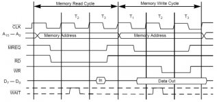
Z80_memory_rw_600.jpg
 
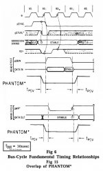
gathered a little info about the S-100 timing when using Phantom [attached diagram below]
since the info was spread about in the manual
I consolidated several bits of the info into one timing diagram
As you can see, the /Phantom signal is supposed to be asserted during the complete memory access, either a read or write
Even though this was taken from the ieee-696 manual,
The controlling logic for /Phantom is still the same for the original S-100, because it is the same function.
As I mentioned in the earlier email, I think the VG ZCB also abuses the /Phantom timing, and not just with the logic circuit.
Since it releases the /Phantom signal much too early.
I've been converting the VG ZCB schematic into the simulator to generate a separate timing diagram to show an overview.

I wondered if you have ever used the ZCB with any other memory card from a different vender [that also supports Phantom] ??
S-100_timing_phantom.jpg
 
I remember from 1978 that the biggest problem getting boards from different companies to work together invariably required modifying Phantom one way or another. It was too loosely defined back in the day. I bet if I walked 50 feet to all my S-100 schematics from the 70s, none would be anything like the IEEE-696 version or even the ZCB version. Some weekend I'll have to get those out and document all the differences between the boards.

The ZCB was an interesting composite board but flip-flop logic... too crude even for that day. And the ZCB should have had a FDC on-board too.
 
... And the ZCB should have had a FDC on-board too.
Not everybody needed an FDC and, considering how many chips it took back then, you probably wouldn't have had room, not to mention compatibility. Cromemco's SCC didn't either; who did make an S100 multi-port Z80 SBC with an FDC on board?
 
I wondered if you have ever used the ZCB with any other memory card from a different vender [that also supports Phantom] ??
I could try it with some Cromemco memory boards, but I think Glitch can also try that himself (and probably already has).
 
I remember from 1978 that the biggest problem getting boards from different companies to work together invariably required modifying Phantom one way or another. It was too loosely defined back in the day. I bet if I walked 50 feet to all my S-100 schematics from the 70s, none would be anything like the IEEE-696 version or even the ZCB version. Some weekend I'll have to get those out and document all the differences between the boards.

The ZCB was an interesting composite board but flip-flop logic... too crude even for that day. And the ZCB should have had a FDC on-board too.

Yes, that's basically the premise we had when we started this discussion
I've had the same experiences with this stuff when the very first new S-100 boards were made.
As mentioned earlier in the thread, we have determined that the reset line being hard wired to the preset pin on the FF is incorrect.
So this is being disconnected and only wired with a pullup.

Glitch did mention on the MARCH group list that he was successful in using other Memory cards with the ZCB
 
Last edited:
Yes, I'm successful with other memory cards -- and even the card I'm working on building -- but only after tripping the POJ flip-flop with a read to somewhere in the ZCB's memory device address space (usually a memory read to 0xE000 from the offboard monitor I'm using). I still need to cut the /PRESET line to the flip-flop and test that theory.
 
glitch said:
...I still need to cut the /PRESET line to the flip-flop...
If you don't want the ZCB to assert /PHANTOM then cutting Jumper C(?) does that.

If your board is socketed you can avoid cutting the trace but reseating the chip in the socket with that signal's pin angled just outside the socket (so it can be restored after your test).

To add a pullup to the line, you should be able to merely solder tack a wire (I use wirewrap wire for jumpers) to a nearby pull-up for a signal that NEVER changes... I think there are a few near the flip-flop.

I assume MARCH is the Mid-Atlantic... group I've seen mentioned a lot the last week or two. I'll check that out on assumption. But if my assumption is wrong, please clarify what MARCH is.
 
Yes, Mid-Atlantic Retro Computing Hobbyists.

I do want the ZCB to assert /PHANTOM in some cases, just not for Power-On-Jump when POJ is disabled. I'm pretty sure it's not actually required to make POJ work, anyway, since the external bus receivers are turned off when internal devices are being accessed (this also prevents DMA from using devices on the ZCB).

The board isn't socketed (factory assembled, only the expensive ICs are socketed), but I may snip the IC's lead on the top of the board and bend it up, rather than cutting a trace!
 
Ragooman said:
...we have determined that the reset line being hard wired to the preset pin on the FF is incorrect. So this is being disconnected and only wired with a pullup...
As a support to Power-On-Reset, I don't really have a problem with this use of /PHANTOM as its being used to access a shadow ROM on start-up; it being used to assure that external memory cards don't respond to the shadow ROM access at the same time. Its an assumption that the board was being used for their product only and to access their shadow rom only, a common assumption at time.

A more complete use of /PHANTOM would be as you said, on the memory access cycle where appropriate, or for such a complete single board computer, just inhibit the memory access from being replicated on the S-100 bus as it serves no purpose. This was more applicable as sbcs became more powerful and not like the original cards that were single function and had to go to the bus for everything.

So for the application which includes another boot ROM that functions independently, I'd just cut jumper C and prevent the board from asserting /PHANTOM. I don't recall from the schematics if cutting that jumper still allows the ZBC to maintain an inactive state signal on the bus which would be more stable than letting it float.

I didn't bother pathing-back the circuitry that releases the /PHANTOM line any further, it looked a little odd and while I was curious, it wasn't worth the additional time.

My vote, cut jumper C to disable /PHANTOM from the ZBC, leave everything else alone. Unnecessary modifications BITE YOU years later when you've forgot what you did, and the schematics no longer apply 100%. Document any changes so you can find them later (I used to tape a note inside my case with changes and useful info).
 
As Glitch mentioned, you still like to use the onboard Rom Monitor [or Ram]. But not with POJ option. I suppose to make Calls from within his code. So you would like to keep the Phantom functionality for any access to that Rom Monitor, especially if your extra Ram card spans 64KB. So cutting just the Jumper C option completely defeats this function. Rather, just disconnecting the reset from the preset pin on the FF and tying this with a pullup avoids the Power On Reset Phantom problem [or any Reset]. And still provides the Phantom functionality for those times you like to access the onboard Rom.

As far as documenting, that's why we have old school paper schematics :)
 
Last edited:
Ragooman said:
...still like to use the onboard Rom Monitor...But not with POJ option...to make Calls from within his code...
The flip-flop only functions on the power-on-reset (POR) as nothing but the PRESET pin can take the Q output high, so there are several ways to disable the POR function as you've described. Maybe the cleanest, self-documenting modifications without a pull-up would be:

(1) Cut the RESET trace to pin 10 of U27 (Flip-Flop) near that pin, ideally on the solder-side of the board.
(2) Solder-jump a short wire on the solder-side of the board from pin 10 to pin 13 of the same chip.

DONE: Now PRESET is tied to CLEAR for that same gate which is already disabled by tying it to VCC.

HOWEVER this PRESET fix, jumpered either way, NEVER INITIALIZES the flip-flop to a known state during power-up. The MREQ trigger of the flip-flop clock will initialize it if that's sufficient. Otherwise you have a more complex mod to change the RESET signal from PRESET to CLEAR instead, which is normally pulled to VCC and might not be an easy cut.

(1) Cut the RESET trace to pin 10 of U27 (Flip-Flop) near that pin, ideally on the solder-side of the board.
(2) Solder-jump a short wire on the solder-side of the board from pin 10 to pin 4 or pin 2 (VCC) of the same chip.
(*) PRESET IS NOW DISABLED
(3) Cut the CLEAR trace to pin 13 of U27 (Flip-Flop) to VCC near that pin, ideally on the solder-side of the board.
(4) Solder-jump a short wire on the solder-side of the board from pin 13 to RESET on pin 4 of U28 (nearby?).
(*) CLEAR WILL NOW INITIALIZE Q ON POR WITH NO /PHANTOM


As to making use of /PHANTOM for shadow rom access:

The other way to assert /PHANTOM that I guess you're referring to is the other pin on the NOR gate U28 which uses jumper pad F. I haven't looked further upstream into that circuit... so as long as the ZBC's micro accesses its own shadow rom through whatever special control, and jumper F is configured to yank NAND U17 pin 4 or 5 low, you'll get a /PHANTOM signal on the bus to block co-addressed memory.

That would certainly improve capability and options... if that's the way it works. As I don't have a ZCB, I'll dig deeper into the schematics only as requested. :)
 
Last edited:
The flip-flop only functions on the power-on-reset (POR) as nothing but the PRESET pin can take the Q output high, so there are several ways to disable the POR function as you've described. Maybe the cleanest, self-documenting modifications without a pull-up would be:

(1) Cut the RESET trace to pin 10 of U27 (Flip-Flop) near that pin, ideally on the solder-side of the board.
(2) Solder-jump a short wire on the solder-side of the board from pin 10 to pin 13 of the same chip.

DONE: Now PRESET is tied to CLEAR for that same gate which is already disabled by tying it to VCC.

HOWEVER this PRESET fix, jumpered either way, NEVER INITIALIZES the flip-flop to a known state during power-up. The MREQ trigger of the flip-flop clock will initialize it if that's sufficient. Otherwise you have a more complex mod to change the RESET signal from PRESET to CLEAR instead, which is normally pulled to VCC and might not be an easy cut.

(1) Cut the RESET trace to pin 10 of U27 (Flip-Flop) near that pin, ideally on the solder-side of the board.
(2) Solder-jump a short wire on the solder-side of the board from pin 10 to pin 4 or pin 2 (VCC) of the same chip.
(*) PRESET IS NOW DISABLED
(3) Cut the CLEAR trace to pin 13 of U27 (Flip-Flop) to VCC near that pin, ideally on the solder-side of the board.
(4) Solder-jump a short wire on the solder-side of the board from pin 13 to RESET on pin 4 of U28 (nearby?).
(*) CLEAR WILL NOW INITIALIZE Q ON POR WITH NO /PHANTOM

yes, good point, always need to reset all those pesky FF's both internal and external :)
Looking at the board layout in the manual helps in this case to find the points to wire this.


As to making use of /PHANTOM for shadow rom access:

The other way to assert /PHANTOM that I guess you're referring to is the other pin on the NOR gate U28 which uses jumper pad F. I haven't looked further upstream into that circuit... so as long as the ZBC's micro accesses its own shadow rom through whatever special control, and jumper F is configured to yank NAND U17 pin 4 or 5 low, you'll get a /PHANTOM signal on the bus to block co-addressed memory.

That would certainly improve capability and options... if that's the way it works. As I don't have a ZCB, I'll dig deeper into the schematics only as requested. :)

The U17 Nand allows additional shadowing, described in 2.3.2 of the manual, for any other cards with Roms that might be in the system, eg, FDD [or HDD] controllers at say 0xE800 to 0xE8FF. Together with Jumper option 'F' and the jumper option 'I', you can have the CPU card assert the /phantom anytime those Roms are accessed by the CPU. It has some flexibility, either 1K, 2K, or 4K blocks -- but it depends on what the device sizes are mapped via those jumpers [area 'J' 'L' and 'M'] for the onboard Roms. That isn't completely independent from the primary addr decode via U13 for the onboard Rom shadowing. Because the U5 decode is dependent on the U13 decode via U17 to the gate enable pins of U5. So those short memory blocks of additional shadowing has to be within the shadowing address range of the U13 decode.

BTW,
there's a 35yr old typo on that page, pin.1 of U5, 74156 is not a bubble input. Internally this input is inverted. Rather, pin.15 is a bubble input as with pins 2 and 14. This is how it switches banks on that dual decode part, since pin.1 and 15 being tied together. This way you can alternate with the Ram decode onboard. The manual left out that little diddy in their errata paragraph at the end
 
Ragooman said:
...a 35yr old typo on that page, pin.1 of U5, 74156 is not a bubble input...
I tend to trust the signal name for active polarity more than bubbles anyway. You can push bubbles around the circuit in pursuit of clarity but it gets hard to tell that the underlying part is, when taken to extreme. Positive Logic AND is Negative Logic OR etc... duality applied to logic gates... fun fun fun.

The only time I bother with bubbles on gates is when I enter a chip into PADs PCB CAD. Sometimes I do, sometimes I don't. I always name the signal with active state syntax. Sometimes that is more clear as it tells you at a glance what the logic gate is, without first deriving the duality equivalent... that practicality appeals to me more as it can lessen confusion in manufacturing and tech support. Its better for them to get the right part or confirm the right part over understanding the logic flow. And if they're ready to understand the logic flow, they can lean positive/negative logic duality to understand it better. Once the engineer has the logic right, rediscovering that is only necessary for a modification.

glitch said:
Yes, Mid-Atlantic Retro Computing Hobbyists.
Thanks.

glitch said:
...The board isn't socketed...I may snip the...lead on the top of the board and bend it up, rather than cutting a trace!
Sounds good too.

I prefer to keep all modification on the solder-side when possible. Less chance of accidental soldering iron mess-ups and better thermal flow when reheating the solder... less likely to harm the chip.
 
Last edited:
Back
Top