• Please review our updated Terms and Rules here

Build your own PDP 8I, book

Hi All;
Thank You, M-Thompson, "" Are the schematics that you have the latest version? "" As I have stated before, This version is a previous version than the book (ed. 1), the book is LD15 and this is LD12 -- LD14 with memory upgrade and I/O upgrade, bring it up from LD12 which is just the basic Processor and switches..
The book is a totally different Design, but the same function..
As far as I know these are the ONLY set of schematics around, and at least up to the book, these would be the latest version..
"" Has this system ever been built and debugged? "" Look at the Pictures that I sent You, but I think that what was built, was not totally documented, or the Schematics and WireLists are intentionally wrong to encourage Learning Debugging and Logic Design.. Just a guess..
I have been assured by Pbirkel, that, that is not the case..
I have not checked the two WireLists against each other as of yet, But, I do plan on doing so, I just haven't had the Time to copy the Second WireList into a third Notebook and compare the two..
I apologize for being so testy, but the same question has been asked a number of times before and I give the same answer and it's like no one has read my previous answers to the same question..
I am back tonight and will be away tomorrow again, I am working on the Memory Module, making it so it will work with the PDP 8i..

THANK YOU Marty
 
Last edited:
Hi All;

I have Data In and Data Out wired on the Memory and 4 of the higher Address lines wired, eight more to go..
I also have to wire in the Write enable circuit..

THANK YOU Marty
 
Marty,

Will this be 4KW of memory? Did you see anything in the drawings for extended memory? We have the luxury now of using 32kB SRAMS and so it might be nice to have full memory on this machine.

Lou
 
Hi All;
Thank You, Lou for Your questions, This machine is 4KW only, at present, and that was the limit of the design..
So, no they did NOT do any Memory Management on this PDP 8i clone..
I am sure it would be possible, I just don't know anything about it, the implementing of it that is..
So, 4KW is full memory for at least now.. And I used the 2114's because they so well matched the kind of memory that I needed, to mate to this machine and they are something that I have here..
And it seemed to me that since this is a 12 bit word machine using two 8 bit rams is a waste of 4 bits..

THANK YOU Marty
I guess is you had the 2114 1Kx4 devices around in quantity (you need 12 per 4KW field) and don't mind doing all the extra wiring.
A couple of 32Kx8's to make a 32Kx16 memory would have future proof the design, you could always add the memory management later (the field select logic on the PDP-8 is pretty simple).
Not using the extra four data bits (or using some of them for word or halfword parity) is really not a big deal compared to the wiring involved (especially if you ever want to expand your 2114 array to more than 4K).

Don
 
Hi All;
Thank You, Don for Your information..
In kind of answer, Yes, I have the 2114's around, but the Board was mostly already wired, as this is the Board that I had used with the PDP 11/40 to replace the Microrom, which needed 256X4 X14, and at the time this was the closest I had to that.. So, I wired it as a 1KX4 X14, and then I took out two of the Rams and I had my 1KX4 with four banks, since the address lines were already wired.. And I had to take out only one link in each row to convert it from one bank of 7 to two banks of three, with a spare Ram and driver that is not used..
"" you could always add the memory management later (the field select logic on the PDP-8 is pretty simple). ""
I would like to do that, once I get that far in the having the machine workable as a plain 8..
I still have I/O to go as well before I even think of Memory Management..

THANK YOU Marty
 
Another possibility would be to use 2x 32kx8 RAMs and switches to select the active field. With a coin cell battery the RAM contents will stay for about 10 years. Then you could load FOCAL in one field, diags on another, etc. Just select the active field and start the processor.
 
Hi All;
M-Thompson, Thank You for the idea and suggestion..
That sounds like a Great Idea, short of Memory Management, and would be a step in the right direction, before trying to implement the Memory Management circuitry..
I had most of all the address lines hooked up, and then I realized I had forgot to hook in the 7442 to the first two addresses MA0 and MA1, so I need to straighten that out, then it will be hooking up the R/W line to the 2114's..
Then things will be ready for a first test, I will still need to pick the RC combination for the 9602's for the pulse width of the write pulse.. After that we shall see IF I have working Memory..

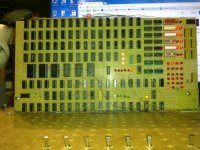
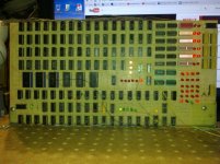
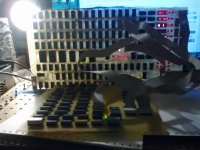
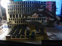
Here a some pictures of the unit, just after I turn it on, it usually comes up with the IR Register all on, and the ALU doing one of a couple of things, either Counting all the way through the ACcumulator Register or as in this case, what is in the ACcumulator Register being shifted to the right all of the way through and including the Link bit..

001.jpg 002.jpg

003.jpg 004.jpg

This is without the Memory Board attached..

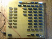
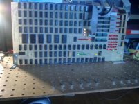
Here is a picture of the Memory Board.. There are alot of Sockets that are no longer used..

005.jpg

THANK YOU Marty
 
Last edited:
Hi All;

I have wired in the rest of what I need, and so far there is NOT any Read or Write..
But, there is much that I need to check..
I am monitoring the Select line, and it is fine as well as the Read/Write line..
But, there are a number of thing to check, including a mod that I was told in the memory re-work to do, which needs checking, it may need to be switched back..

THANK YOU Marty
 
Hi All;

I got the Read to work, now for the Write..
I got Write to work, but automatic advance doesn't work now..
I will need to investigate this more, I had automatic advance working earlier, but not write..
I thought I had them both working, when I was testing the 9602's on a breadboard..

THANK YOU Marty
 
Last edited:
Hi All;

I have found out the "what" but, not the "why" of my mystery of auto-increment..
When bit 04 is set to a one, then I can auto-increment when it is set to zero then I can't auto-increment..
My understanding is when this bit is zero, then Page '0000 is addressed and when it it set to a one some other page is addressed..
And this is where it hangs, it is for some reason, trying to look for an indirect address at state 7, when it is at "zero" and it should not be doing so..
And somewhere here is the problem..
So, I'm glad I found something, not the solution, but, at least I know in what area to look for the problem..
Well, even that doesn't work now, and I have switched back to the 7489's and it does the same thing, so either I have a Bad IC, or a mis-wire..
I am going to check out what I have fooled out with and the Deposit and Examine circuitry..

THANK YOU Marty
 
Last edited:
Hi All;
I think I have something, I found while checking different Ic's, that having G8, a 7474 in the Automatic incrementing doesn't work, but taking it out, it does work.. And it's output is the Clock for the MA Register, So I will check Both the upper and the lower MA Ic's, F12 and F13.. And make sure they are wired correctly, and while converting to the other memory Board, I didn't mis-wire something by mistake..

I have a picture of it doing something, I am NOT saying it is correct, just interesting..
And for You viewing pleasure It is Incrementing three of the Registers at the same time.. The AC, the IR and the PC Registers all Increment the same..

001.jpg

THANK YOU Marty
 
Hi All;
The Write circuitry wasn't correct for the 7489's and the addresses for the MA 8,9, and 10 was not connected for the 7489's..
So, now I can again try the Memory Module and see if it will work..
I have the Memory Module working with Read and Write..
Auto-increment still does not work, when all of the instruction Register is cleared.. I have to find out which ones to turn on to make it work, if all are on then Auto-increment works..
I am also going to try and finish documenting the other wire list and comparing what the differences are and whether I need to implement them..
I also need to figure out "why" if I put something in memory, when I 'press' the CONTinue button that it isn't copied to the IR Register.. Lots to do..

THANK YOU Marty
 
Last edited:
Hi All;

I have a Question ---

The way I have it wired at Present to Determine which Page is used for Memory Access PC04 is used to Determine whether it is page '0' or another page.. And if PC04 is a '1' then PC0 thru PC03 are used for the Page adderss..

BUT, in the other WireList, MB0 thru MB04 are used instead..

So, which is Correct, I have the PC0 thru PC04 wired in at present ??

THANK YOU Marty
 
Hi All;

I am going to change four timing connections, per the other WireList and see if that makes any difference in what it does.. Especially I am interested to see if this helps or fixes the problem of Memory Data going to the IR Register..
And after that since I have had No response to my last posting, I will try changing the PC00 thru PC04 to MB00 thru MB04..
If nothing else that May fix my Memory hanging, as described above..
All of these changes are per the other Listing, and after a closer examination, there may be more changes..
Changing the four timing connections, fixed the Memory Hanging problem, but it didn't fix the Memory to IR problem..
I am next going to change the PC to MB and see what this does to the machine..

THANK YOU Marty
 
Last edited:
Hi All;

It looks like I have to hook back up one of the A0 connections.. The other two I have not completely investigated..
I have to look at and put on paper the equations for the ALU Instructions, as it looks like when CP0 timing is issued, it doesn't respond to the correct set of settings during the F1 timing, as shown in the Diagrams.. And, so NO Loading of the IR Register at the F1 time.. I can't explain it, but I know what I need for it to work..

THANK YOU Marty
 
Hi All;

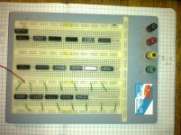
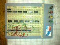
I have made the preliminary design for the ALU control circuitry, and will be wiring it up on my Breadboard, and testing it before wiring it up permanently on the Wirewrap Board.. And even if I find the origonal problem, this is good exercise for me..

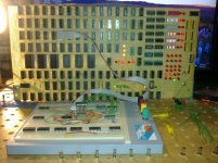
Here is a picture of the Bread Board, only the lower 5 Ic's are going to be used..

001.jpg 002.jpg 003.jpg


As You can see it is all wired in, it's not working correctly, but there is much to check.. Like wrong wire, no wire or too many wires, and to make sure the polarity is correct on each control bit..

THANK YOU Marty
 
Last edited:
Hi All;

Last night after going to bed, I found a couple of things..
One is a wrong connection, because I copied it wrong, I copied OPG1 where it should have been OPG2.. And on two of the output Ic's It needed to be a NAND gate and I had a NOR gate.. For the signals M and S3, so I can fix that as well.. And maybe also I will need to do the same for S0 thru S2, because of added equations..
This is why I have learned to do it first on a BreadBoard, and work out the kinks..

THANK YOU Marty
 
Last edited:
Hi All;

I have re-attached the S0 thru S2 of the original circuit and will re-wire up the circuit, I have for M and S3, and until I get those two working, I will not try any of the others.. Then I will proceed with the rest of them one at a time.. And if I have to I will do M and S3 separately, but they should be fine.. As I had previously wired up M and had it working, not in this last wire up, but the one before that..
I have M working, S3 has a problem.. I had to try them separately..
I have M and S3 working, next is S2..
I now have S2 and S1 working and I can also now put an instruction into Memory, using the 7489's and it shows up in the AC register, (I am not saying that this is correct), but next is S0 and I can then see if it will show up in the IR register..
No, it does the same thing..
I found a major problem and I fixed it.. The Strobe pin on the 74150 was Not connected to Ground, So, it would not do it's thing and so once I grounded it, things started to work more correctly !!!

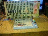
001.jpg 002.jpg

003.jpg

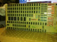
Unfortunately, you cannot see the row of Green led's that show the status of what I got going..

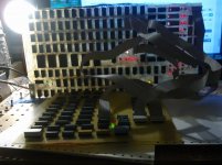
001.jpg

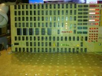
This is a picture of it with the Memory Board behind the main Board, even though you cannot see much of it..

THANK YOU Marty
 
Last edited:
Back
Top