• Please review our updated Terms and Rules here

Yet another T11 project

md95065

Member
Joined
Jun 1, 2015
Messages
28
Over the last few months I finally got around to something that I have been meaning to do for many years - building a small single board computer base on a T11.

The board has 4 x 28 pin sockets that can support up to 64k of static ram and 64k of eeprom with address decoding handled by a 22v10 GAL that allows a lot of flexibility about what gets mapped where.

There are also 2 x 40 pin sockets for DC-319 serial ports and a 40 pin header for a compact flash card in an ATA bus adaptor.

Interrupt encoding etc is handled by a second 22v10 GAL.

I haven't finished wiring up the ATA bus connector or the interface logic yet, but the processor, memory and serial ports are all working.

The ultimate goal of this is to be able to run the original RT-11 version of Adventure and, possibly a few other games.

While the board should be able to run "real" RT-11 once a suitable driver for the compact flash card has been written it appears that the Mentec license doesn't apply to running RT-11 on "real" hardware so I will probably end up writing my own small monitor program that supports just enough to be able to load and run simple binaries.

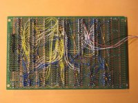
Here is the current state of things:
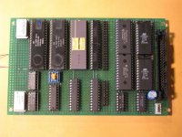
t11_front.jpgt11_back.jpg

I can supply more details if anyone is interested.
 
My first question is where does one get DC319 DLART chips? My DCT11-EM has one on it. Otherwise do they have to be scavenged off other boards?

Do you at some point plan to make a run of PCBs?

Have you seen CHD's work on an ATA qbus adapter? Chuck did write an RT-11 handler for his design. Maybe that will help you a bit. See here: http://www.chdickman.com/qbus_ide/

I was thinking of building one of Chuck's boards. It was the programming of the PLD that was holding me back, since I don't own any hardware to do it.

Lou
 
My first question is where does one get DC319 DLART chips? My DCT11-EM has one on it. Otherwise do they have to be scavenged off other boards?
The DLARTs are "borrowed" from a Falcon board (as is the T11).

It occurs to me that one could probably construct a DC319 compatible device from some kind of PLD and, possibly, a microcontroller, that would fit into a 40 pin DIP footprint but I haven't thought about it in detail.

Do you at some point plan to make a run of PCBs?

Possibly. I suspect that the most useful thing for most people might be a 2 card set rather than a single board - one that has the CPU, memory, address decoding and interrupt logic and a second one that was purely for i/o devices - then if people wanted to use something other than the DC319 they could still use the main CPU board.

Have you seen CHD's work on an ATA qbus adapter? Chuck did write an RT-11 handler for his design. Maybe that will help you a bit. See here: http://www.chdickman.com/qbus_ide/

Yes, I saw that years ago when he first did it, but I had forgotten that he had also written an RT-11 handler for it - thanks for reminding me.

I was thinking of building one of Chuck's boards. It was the programming of the PLD that was holding me back, since I don't own any hardware to do it.

If I wanted to build one of those things now, I would probably use discrete components for the bus interfaces and device registers and hook it up to an Arduino board or something similar.
 
I would be interested. By the looks of it you are using the T11 in 16 bit mode, I was thinking of going 8 bit mode and doing a really minimal system (a bit like the schematic on page A-59 of the T11 manual). Like yourself I was thinking about doing a minimal monitor.

Still thinking about the best way to do serial. So far leaning towards trying something with an 16550 or so, but even those aren't so easy to come by nowadays.

By the way, T11 chips are available here:
http://www.arclightindustries.com/store/node/2
 
As it turns out there is a monitor for the T11 evolution board, it's printed in the back of the manual. The MESS emulator project seems to have ROM images, but they do not appear to match the listing.

Is anybody aware of someone having OCR'ed or otherwise reconstructed the MACRO11 listing from the DCT11-EM manual?
Is anybody aware of good rom images of this board?

That evaluation board also gives another idea for serial: the 8251 USART, which still seems available as NOS on eBay.
 
Yes, my board is a 16 bit system - I did consider just doing 8 bit but it really isn't much effort to add the extra sockets and wiring for 16 bit memory and it seemed to be worth it for the performance gain.

What serial chip you use is really a matter of personal choice - almost anything could be made to work but, if you want to end up with something that looks like a DEC serial interface with even a minimal implementation of the control and status registers I would be looking for something really basic, like the AY-3-1015D, where all of the interesting signals are exposed to the outside world rather than being hidden inside the chip in various registers. It looks as if things like the AY-3-1015D can still be found on eBay from a few sellers.

As far as the DCTEM monitor is concerned, you are in luck. When I first got my DCTEM board, many years ago and long before the manual showed up online I disassembled the entire monitor, and spend quite a lot of time annotating it. The result is something that you can assemble with MACRO11 and get back to the identical binary bits that are in the ROMs on the board. There are a few obscure bits of code, such as the expression evaluator, that are pretty much uncommented and there are probably quite a few places where my interpretation of the code is just wrong, but referring to the "real" source code in the manual should resolve these issues.
By the way, the listing in the manual is for exactly the version of software (I suspect that there was only ever one version) that is on my board - the checksum (which is embedded in the code) is identical. Unfortunately it looks like I can't just upload the file as an attachment to this message so I will have to find another way to get it to you.
 
Thanks all for your input!

@md95065: thanks, I've PM'ed you with my e-mail address.

@Lou: if I understand the listing correctly, both rooms must end with a 010 byte, indicating version 1.0. The images I found end with some 10...20 zero bytes. With the recreated source available I guess rom images have become moot.

Just to give you guys an idea where I'm coming from:
- my interest from back in the day is the TI990 and the PDP11. The two are architecturally very similar, with some interesting differences.
- a few years back I built this project (a design by stuart conner): http://www.avjd51.dsl.pipex.com/tms9995_breadboard/tms9995_breadboard.htm (the 9995 is to the TI990 mini what the T11 is to the PDP11).
- this evolved into a breadboard with a CF card "disk": http://ruizendp.websites.xs4all.nl/board.jpg
- and finally into this: http://ruizendp.websites.xs4all.nl/IMAG0266.jpg
It runs Forth, Basic, a CP/M like OS "MDEX" and LSX unix; still working on some other operating software.

For me a T11 project is a compare and contrast thing. Will probably try to begin with something simple and gradually build out, for instance, starting with 8-bit on a breadboard and then 16-bit on a pcb (i.e. something very much like you are already building).

Also found a 12 year old project by Peter McCollum, including MACRO11 source for its Fig-Forth operating software (closely based on the PDP11 version):
http://web.archive.org/web/20091026230444/http://geocities.com/saipan59/dec/t11.jpg (schematic)
http://web.archive.org/web/20091026230441/http://geocities.com/saipan59/dec/fsa.txt

Will look into your suggestions for a UART.

Will you post schematics for your system?
 
Hi All;

PNR, I am an old TI 990 fan, I worked with both the 990/10 and the 990/12 for many Years, Testing various boards that the company I worked for manufactured.. Was the 9995 what was used in the 990/10A ?? I don't Remember any more..

THANK YOU Marty
 
@md95065: thanks, I've PM'ed you with my e-mail address.
Thanks, I will respond to that later today

@Lou: if I understand the listing correctly, both rooms must end with a 010 byte, indicating version 1.0. The images I found end with some 10...20 zero bytes.
OK, I understand the confusion - something rather non obvious is going on here ...

The ROMs occupy the address range from 120000 - 157777, but the highest order address line going into the ROMs is inverted, which means that:

offset 000000 - 017777 in the ROMs corresponds to addresses 140000 - 157777
offset 020000 - 037777 in the ROMs corresponds to addresses 120000 - 137777

So, the version number that you were expecting to be at the end of the ROM is actually right in the middle of the ROM at offset 017777.

(By the way, I can find no evidence on the DCTEM schematic to indicate that signal - SAL13 - being inverted before it gets to the ROM, but that is the only explanation that I can come up with for why the contents of the ROM are arranged in the way that they are)

Will you post schematics for your system?

Yes, schematics will be available soon.
 
Last edited:
DCTEM monitor disassembly

DCTEM monitor disassembly

Well, it looks as if I can attach ".txt" files to a message, but only if they are less that 48.8k in size ... :confused:

So, here is the file split into 2 parts.

I hope that this isn't a breach of Forum etiquette ... (apologies in advance if it is, but I couldn't find anything that prohibited posting things like this)
 

Attachments

  • dctem_part1.txt
    40.3 KB · Views: 6
  • dctem_part2.txt
    39.3 KB · Views: 4
Was the 9995 what was used in the 990/10A ?? I don't Remember any more..
I've replied to your question more fully in a separate thread:
http://www.vintage-computer.com/vcforum/showthread.php?49301-TI990-minis

In short: no, the 990/10A was powered by the 99000 chip. Think of the 9995 as roughly equivalent to a T11 and a 99000 as roughly equivalent to a single chip F11. However, the 9995 and 99000 share much of their design. In some very simplistic testing the 9995 comes out about as fast as a PDP11/40. Part of my interest is in getting a feel for the speed of a T11, I think it will be about the same. The 99000 was about twice as fast.
 
Schematic

Schematic

Since several people have asked for it, here is a link to a rough version of the schematic.

This was my first attempt at entering a schematic into KiCad, so it is still a bit of a mess - in particular you should ignore the component numbering and be aware that the two DLART chips and the IDE bus connector are not shown - they should be on a second sheet (which doesn't yet exist).

This should, however, be enough to get an idea of what the thing consists of and I think that most things should be pretty much self explanatory.

The processor is clocked at its maximum frequency of 7.5MHz. Since 7.5MHz crystal oscillators are hard to find, I used a 15MHz oscillator and used half of a 74S74 to divide it down to 7.5MHz (the schematic says 74LS74, but it really is a 74S74) - the S74 was used to keep the clock waveform as symmetrical as possible since the processor is being run at full speed and requires that both the clock high and low times are > 60ns (LS TTL low-to-high and high-to-low propagation delays are sufficiently asymmetric that, if an LS74 had been used we might have been running quite close to that limit).

Addresses are latched by 2 x 74LS573 (actually 74HCT573 in the prototype).

Address decoding is done by a 3 input NAND gate and a 22V10 GAL. The NAND gate decodes a "bank 7" signal from A13, A14 and A15 and A3 - A12 are input directly into the GAL, allowing us to decode addresses all the way down to an 8 byte block. (The bank 7 signal isn't really necessary but generating it externally gives us 2 extra spare inputs on the GAL, and I already needed a 3 input NAND gate package for other reasons). The GAL outputs chip select signals for the various components, along with a -RDY signal to extend the bus cycle for slow devices (the DLART spec suggests that they need this when the processor clock is 7.5MHz as it is here), and a RD_ENABLE (read enable) signal which feeds into the read/write logic and makes it easy to define blocks of addresses as being "write only" at the h/w level - this is useful for devices that don't like the way that the T11 always reads from a location prior to writing to it.

Read and write strobes are generated by a 3 input NAND gate and 3 x 2 input OR gates which gate the strobes with -CAS.

The other GAL deals with interrupt encoding, interrupt acknowledge decoding and loading the mode register on power up. Interrupt and halt signals are latched into a 74LS574 on the leading edge of -CAS and the GAL outputs the priority encoded interrupt data on CP0-CP3. The GAL also takes RAS, SEL0, SEL1 and DAL8-11 as inputs so that it can generate interrupt acknowledge signals. The only device that needs an interrupt acknowledge is the LTC (line time clock) interrupt. The LTC comes from one of the DLARTs and clocks a high level into a 74S74 latch. The output of the latch feeds into the 74LS574 interrupt latch mentioned above, and the IACK_LTC output from the GAL is used to clear the 74S74 LTC latch when the interrupt is acknowledged by the processor.

The mode register configuration is set up for 16 bit mode, normal read/write timing and a start address of 172000, which requires asserting DAL8 and DAL11 low when -BCLR is asserted. Since DAL8 and DAL11 already need to go to the interrupt decode GAL anyway, they are assigned to i/o pins and a low active BCLR signal is also input to the GAL allowing it to handle mode register loading.

As previously mentioned, the two DLARTs, their associated crystal oscillator and the IDE bus socket are not shown.

The GALs were used purely to keep the component count down to a level where it was possible to construct the prototype on a 100mm x 160mm eurocard sized board - they only contain very simple combinatoric logic which could easily have been implemented with discrete TTL components at the expense of using more real estate on the board.
 
Also found a 12 year old project by Peter McCollum, including MACRO11 source for its Fig-Forth operating software (closely based on the PDP11 version):
http://web.archive.org/web/20091026230444/http://geocities.com/saipan59/dec/t11.jpg (schematic)
http://web.archive.org/web/20091026230441/http://geocities.com/saipan59/dec/fsa.txt
Hi, that's me.
See the recent thread:
http://www.vintage-computer.com/vcforum/showthread.php?47569-T11-clock-running-Forth
The PCB that we made recently is essentially the same as that 12-year-old hand-drawn schematic.
Pete
 
@md95065:
Thanks for that info, and yes the MESS images are indeed organized as you describe. Checked the schematics again: indeed the inverted address line does not appear. I noticed that almost 3KB of the 8KB ROMS are unused. Perhaps they first planned on using 4KB ROMS and SAL13 was used as part of an address decode and this remained on the PCB when the ROMS were enlarged ??

@saipan59:
Thanks for that link, most interesting and a great board! I'm not entirely sold on the idea of an 6850 and under clocking the T11, but that is nitpicking.

So, my current thinking for a breadboard system is:
- T11 in 8 bit mode, running at (close to) full speed
- 64KB RAM, 32KB ROM (ROM can be banked out to reveal other half of RAM)
- UART + USB-serial bridge
- CF Card (in 8-bit memory mode, very easy to interface)
- minimal glue logic

I guess the ROM could hold both a DCT11-EM derived monitor and FigForth. The derived monitor would allow for download of binaries (similar to the HOST command, but using the same UART). That setup should allow loading and testing of RT11, and of LSX unix. I don't have a working MX unix yet, but that should be possible as well.

A PCB version would then upgrade to 16-bit mode and to use of CF card via an IDE converter board. Eurocard sized PCB's with solder mask and silk screen from China are about $20 each even in small (3+) series.

So much for vision: from my perspective, this is a two year plan in many small steps. Perhaps md95065 will have a PCB version done well before I even get to do a breadboard version :)

Now for some very practical questions:
- As I understand the T11 manual, it always does a read before write, in any memory mode. Is that correct? Why is this so?
- Are 6850 UART chips still easy to get?
- Has anybody considered the 6551 UART?
- Wikipedia says that RT11 came with uncommented source code, so that versions with other device drivers could be sysgened. Is that correct, has this source survived?
- It also says that the documentation had a commented source code listing, but I did not see that in the documentation on bitsavers. Is Wikipedia correct, has this documentation survived?
 
Yes, read before write is true. Don't know why.
6850 UART: Don't know how common, but I had a bunch of them to share with folks on my PCB build. My implementation with it was not trouble-free - probably missing a bit of glue logic to make it work better.
I probably considered the 6551 years ago, because I have some of those also, and I used to do a lot of 6502 stuff. I assume it's cheap and easy to get.

Pete
 
Yes, read before write is true. Don't know why.

It is for "hardware minimization" - ie making the processor logic for dealing with destination operands simpler (and, therefor, smaller).

The majority of those operands are read-modify-write, a few are read-only, but only two (that I can think of) - MOV and CLR are write-only.

The original LSI-11 did this as well, and used a DATIO(B) bus cycle for the destination operand of MOV and CLR instead of DATO(B).
 
Once again: thanks all for sharing!

@md95065: I remain very interested in your project. Let me know if I can be of assistance with the CF interface or PCB design. I don't have DC319 DLART chips, so that part will remain a challenge for me.

@saipan59: later this year I'll experiment a bit with UARTs and see if I can come up with something not too finicky with a readily available period part.

I hope I have not "hijacked" this thread too much over the past days.
 
I just noticed this thread. I have both a T11 chip and the DLART chip that I got as samples many years ago. I worked for Digital from '77-'80 at the Maynard Mill, and I worked on many LSI-11 projects in the eval group. I might have had my hands on a Falcon board once before I left. I'm considering building a computer with these chips. I would add a memory management unit using a 74hct612 that I also have. I think I could route the "fetch" status as one of the four map address inputs to separate the memory into I space and D space. The biggest challenge will be to get the source for the ODT firmware assembled and burned into rom. I'm trying to use the GNU gcc assembler to build the MACRO-11 sources, but translating the syntax is stumping me. BTW, the DLART chip can be replaced with an AY-3-1013 or similar uart, a baud rate generator, and some glue logic if you can live with plug settable baud rates.
 
Back
Top