• Please review our updated Terms and Rules here

Identify the DOS ROM chip in 8088 laptop

AlexC

Experienced Member
Joined
Jun 26, 2015
Messages
275
Location
Germany
Hi,

As per this thread, I've been trying to gain access to the 'expended' (as the BIOS calls it) 128KB RAM to use as a RAM disk.

SI from Norton 4.5 shows 128KB of extended RAM at 10000-12000. No other memory tool that'll run on this machine sees it, and I can't run himem.sys on an 8088, but vdisk.sys from DR-DOS can find it and use it as a RAM drive. I can write to the drive and read back what I've written, but after a minute or so the contents get corrupted.

I'm pretty sure this is due to that 128KB sharing address space with the 128KB DR-DOS ROM disk that's embedded in this machine, which it will boot from by default. Since DR-DOS 3.41 is not much use to me and I have bootable floppies (this machine has no hard drive), I'd like to disable the ROM disk and use the 128KB as a RAM disk.

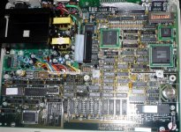
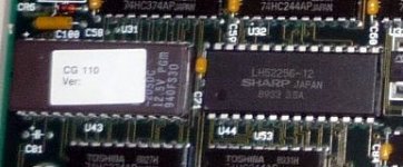
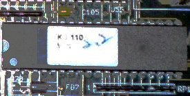
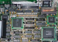
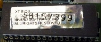
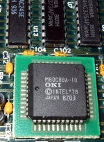
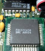
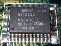
There are three ROM chips on the board. One is the Award BIOS and is removable. The other two are not removable, shown in the photo with white stickers on them. I don't want to damage either of these irreparably, so I'd like to identify the Vcc line and carefully snip it. Does anyone have any idea which chip that would be, and which leg(s)?
 

Attachments

  • Veridata.jpg
    Veridata.jpg
    103 KB · Views: 1
An old laptop which boots DOS from ROM is pretty neat and rare on it's own, is it worth the effort for a tiny RAM disk?

Check the model numbers on the ROM chips. I think the chip with a sticker on the right hand side of the photo is actually the keyboard chip.
There is also another chip at U44 which I suspect may also be a Mask ROM, I'd check it's model number too.

The giveaway could simply be the size - a 128KByte DOS ROM is likely to be either a 1Mbit ROM or maybe 512KBit if they compressed it. Where as the system or video stuff will happily fit on standard 2764/27128/27256 parts.
 
I can't be 100% helpful here - just replying hopefully in time to stop you from trying to clip the power pin to one of the chips, as that won't help at all. Removing the power from a chip does not remove it from the circuit, in fact it is more likely to load the address and data lines like a dead body lying across power lines. Nothing but trouble.

First, if you have the tools and the skill to do it carefully remove the chips in question and fit sockets. Now, you can disconnect any pin by bending it carefully out horizontally away from the socket before you plug the rest of the pins into the socket.

If you really can't take the chips out the the proper way to remove a memory IC from circuit (in-circuit) is to leave it powered and snip its _CE pin close to the PCB so there is a still a reasonable length of leg left attached to the ROM. Take that high (ie, to 5V) to make the chip effectively vanish from the address and data lines. The forum SW has shrunk your picture to such an extent that I can't really see how many pins the devices have, so can't suggest pin numbers.

Of the two white labelled devices, the one at the left side looks like it really is a ROM: The device on the right is more likely to be a microprocessor with a built-in code eprom, like an 8748 or 8751, or similar. As such, the lines going in and out of it will nearly all be control lines for one purpose or another.

Isn't there a more elegant way to disable this onboard DOS feature? A setting in the BIOS, or a jumper link on the motherboard?
 
Thanks, both of you. As far as I can tell there's no way to disable the ROM boot but I'd love to do it non-destructively if possible. The trouble is I can't find anything about this laptop online: Veridata TurboLite 110. A couple of photos and some German stuff about a non-booting hard drive, that's all.

The boot from ROM is annoying because there's no way to modify config.sys or autoexec.bat, so it just boots to 'time, date' commands. To get it to boot from floppy you have to press 'F' at the right time (too soon and it complains of a stuck keyboard, too late and it boots from ROM). DR-DOS is glitchy with the software I want to run on here, but I have good MS-DOS 3.30 floppies that do everything I want. An extra 128KB of workspace would be useful, though not essential.

The laptop also has an empty ROM socket in the back, behind a drop-down flap. I think that's for a DOS upgrade, but I've no idea where I'd find the right chip. It would be interesting to put my own config on an EPROM and plug it in, but without more specs I wouldn't know where to start.

Slightly better photos attached, hopefully.

Edit: looks like the Sharp chip is CMOS static RAM.
 

Attachments

  • 01.JPG
    01.JPG
    20.9 KB · Views: 1
  • 02.JPG
    02.JPG
    14.7 KB · Views: 1
Last edited:
Yes, the sharp IC is an SRAM. The smaller labelled chip looks to me like an EPROM although the part number is covered - without any prior story or input from you I would have assumed that the 'CG' in 'CG 110' would mean 'character generator'. The larger white labelled chip looks to be 'K<something>110', and if I were a betting man I would guess that the <something> is 'B', so 'KB110', strongly suggesting that this is a microcontroller programmed as the keyboard controller, as was already suggested.

I've just noticed that part of the PCB number along the bottom edge in your original picture is 'TL110', so that's what I think the '110' part of the numbers of the chip labels are referring to -

small chip = 'character generator for type 110 PCB'
large chip = 'keyboard controller for type 110 PCB'

(I'm just guessing, obviously).

Could your DOS be elsewhere on the board? In non-windowed ROMS or PROMs? Could it even be built into the Award BIOS?
 
Last edited:
Interesting, thanks. I was wondering what the 'CG' might stand for. And that makes sense re 'KB' too. There don't seem to be any other large chips on the board except what you can see in my main photo. There's nothing under the black box in the top-left - that's the housing for the battery.

Here's a better photo of the top-right. You can see the ribbon cables going to the back of the casing, where a user could plug in an addition ROM chip.

I don't suppose the DOS ROM drive could be stored in the system BIOS chip too, could it? Would there be room for the Award BIOS and the 128KB DOS ROM?

(Heh, I wrote that before seeing your edit: "Could it even be built into the Award BIOS?" - so at least two of us think it might be possible!)

If not, I'm kind of stumped. I won't take snippers or soldering iron to this without knowing exactly what the results will be. It's a pristine machine - I could believe it's never even been used - so I won't do anything that's irreversible. But it would be nice to get that 128KB back and have an automatic floppy boot.

Edited to add photo of Award BIOS chip.
 

Attachments

  • BIOS.jpg
    BIOS.jpg
    97.9 KB · Views: 1
  • P1000451.JPG
    P1000451.JPG
    29.4 KB · Views: 1
I think if the DOS was in the BIOS IC it would have a copyright message on it about that in additional to the AWARD copyright message. Also I agree, 128K is a bit small for a BIOS and an OS combined.

The Faraday chip produces some hits variously as a 'chipset' chip or bus and peripheral controller, so we can probably rule that out.

The square SIS chip - what I mostly remember SIS for originally is graphics hardware, but a search on SIS 83C747 produces one hit vaguely suggesting it might be a multi-io controller chip - the sort of chip you might have found on a plug-in serial / parallel port card at one time - so this is probably providing the board level I/O functions (there will be buffers or level converters in between this IC and the actual COM and LPT ports).

The square OKI chip I still can't quite read even if I save your image and zoom into it in an image viewer - the main part number looks to have a '-<two digits>' suffix which strongly suggests it might be a memory device of some sort, with the -nn designating the speed, as also usually found on RAM and EPROM ICs. What's the part number on that chip?

Also, on the original image, what's the part number on the large rectangular surface-mount chip near the board edge, south of the CG Rom and the RAM?
 
Oh, One other thing: It's not obvious from your photos how much space there is between the power supply PCB and the main board underneath. Have you looked underneath the power supply yet?
 
Here are some more photos. I think we have an 8088 CPU, an SMC floppy disk controller and a Yamaha display adapter (this laptop can handle CGA on the LCD screen, CGA or MDA/Hercules on an external monitor).

And having had another look, that other white-labelled chip is definitely 'KB 110'.

As for the board, it's an optical illusion - there's just one plane. The PSU components are all on the same level.

I did find this which mentions an 'Award card' when building a DR-DOS ROM disk.

I guess the idea was for this machine to be sold as it is now, then various ROM packs made available with upgraded operating systems for users to plug into the socket in the back. It would be nice to build my own bespoke bootable ROM disk, but even with an EPROM programmer I wouldn't know where to start.
 

Attachments

  • DSCF0276.jpg
    DSCF0276.jpg
    92.8 KB · Views: 1
  • DSCF0277.jpg
    DSCF0277.jpg
    83.8 KB · Views: 1
  • DSCF0278.jpg
    DSCF0278.jpg
    77.9 KB · Views: 1
...
I don't suppose the DOS ROM drive could be stored in the system BIOS chip too, could it? Would there be room for the Award BIOS and the 128KB DOS ROM?
....

The BIOS chips has 32 pins, so it could be any of a 512k-bit to a 4M-bit (64K Byte to 512K Byte); you'd need to peel the sticker up a bit to see what part number it is. It would be very easy to fit everything in a 2M-bit (256KB) chip. It could even be a 512KB chip with some bank-switching going on to access four banks of 128KB.
 
Thanks, I'll take a look next time I dismantle the machine.

Given everyone's feedback so far, I'm fairly convinced the ROM disk is sharing the BIOS chip. Modifying that is way beyond my level of expertise, so I guess I'll just stick with pressing 'F' at boot time and not worry about the 'lost' 128KB.

Thanks all: it's been very educational.
 
If you decide to come back to it later, you can get EPROM programmers cheap off ebay - and you could read the contents of that chip to find out. Then potentially a replacement could be written to a blank EPROM that had the DOS part removed (assuming you found DOS in it).

I get the feeling that is where DOS sits too, because 1Mbit seems a little beefy for just an 8088 BIOS.
 
Well, here's a crazy idea: Would you say that you have to press 'F' at exactly the same point (in time) after a reboot in order to bypass the onboard DOS? If so, how about:

A little add-on circuit which detects when the reset line comes out of the reset state... waits for exactly n seconds... then drives an optocoupler LED on for n seconds... then turns it off again.

Connect the optocoupler transistor (with appropriate collector / emitter polarity) across the 'F' switch connections on the keyboard so that the circuit can 'press' the F key.

This little AUTO-F circuit will then always automatically bypass the internal DOS for you after a reset or a power-on. Harder to say what it would do after a soft reboot though: That depends on what happens to the uP reset line in those circumstances.

If I was going to do this I would use an 8-pin PIC chip like the PIC16F629 to do the timing because that's something I'm familiar with, but you might prefer to do it with a dual-monostable logic IC or some other microprocessor - I'm not familiar with the physical layout of your machine but you could probably make this after-reset-F-press-circuit small enough to hide out of sight somewhere.

The real appeal of this idea for me is that it doesn't require you to do any hacking of the original firmware or remove, damage or change any of the original parts - you just add a little circuit to make the machine more convenient to use and then remove it whenever you want to return it to absolutely stock condition.

Oh, incidentally - the proximity of the 'CG110' EPROM to the chip you have now identified as the graphics IC makes the EPROM even more likely to be a character set (character generator) ROM.
 
Last edited:
If you decide to come back to it later, you can get EPROM programmers cheap off ebay - and you could read the contents of that chip to find out. Then potentially a replacement could be written to a blank EPROM that had the DOS part removed (assuming you found DOS in it).

I may buy an EPROM programmer anyway as it would be useful for some other projects. There's no harm in having a play, but I doubt my ability to find exactly where the DOS bit starts and, even if I did, disable it without inadvertently preventing a clean boot.
 
Well, here's a crazy idea: Would you say that you have to press 'F' at exactly the same point (in time) after a reboot in order to bypass the onboard DOS? If so, how about:

A little add-on circuit which detects when the reset line comes out of the reset state... waits for exactly n seconds... then drives an optocoupler LED on for n seconds... then turns it off again.

Connect the optocoupler transistor (with appropriate collector / emitter polarity) across the 'F' switch connections on the keyboard so that the circuit can 'press' the F key.

This little AUTO-F circuit will then always automatically bypass the internal DOS for you after a reset or a power-on. Harder to say what it would do after a soft reboot though: That depends on what happens to the uP reset line in those circumstances.

If I was going to do this I would use an 8-pin PIC chip like the PIC16F629 to do the timing because that's something I'm familiar with, but you might prefer to do it with a dual-monostable logic IC or some other microprocessor - I'm not familiar with the physical layout of your machine but you could probably make this after-reset-F-press-circuit small enough to hide out of sight somewhere.

The real appeal of this idea for me is that it doesn't require you to do any hacking of the original firmware or remove, damage or change any of the original parts - you just add a little circuit to make the machine more convenient to use and then remove it whenever you want to return it to absolutely stock condition.

Oh, incidentally - the proximity of the 'CG110' EPROM to the chip you have now identified as the graphics IC makes the EPROM even more likely to be a character set (character generator) ROM.

That's such a wonderfully Heath Robinson idea that it appeals to me immensely!

The warm boot time is significantly shorter than the cold boot time, which may scupper things.

I don't think I currently have the electronics/soldering skills to do this, but it would be a nice project by which to learn them.
 
- Unfortunately this is way out of my experience because I used an Atari ST as my main computer all the way through the early PC period so I don't know much about 8088, but -

It should be possible to explore the content of the BIOS eprom without taking it out. The processor is clearly able to get at the code in the BIOS eprom - if it couldn't, it wouldn't be able to run the BIOS code.

You might be able to write - or you might be able to find - a utility which will read through the content of the BIOS eprom area and dump it to a file for you to have a look at, or you might even be able to view it just by using a common or garden memory browser / debugger / disassembler program pointed at the right address range. Programs like this also usually show the memory content not only in hex form but in ASCII as well, useful for finding plain text words which might clue you in to what it is you're looking through.

A nice old book that I have here in my collection - "PC INTERN SYSTEM PROGRAMMING" (Abacus, 1994) suggests that the address range C000 to FFFF would be a good place to look.

Apparently the end of the BIOS will normally be found at the last address in that range, FFFF, but the start address varies with the size of the BIOS code. The original IBM PC Bios started at E000. From C000 onwards is where you may find other ROM extensions, perhaps even that elusive ROM based operating system you've been looking for.
 
you can get EPROM programmers cheap off ebay

Can you provide one or two links as examples? I've been looking for one recently and I can only find programmers around the $100 mark, and many of them are SPI only. I haven't been able to find any cheap parallel (PC EEPROM type) programmers at all. Hopefully I'm just searching for the wrong thing...
 
I've been looking for one recently and I can only find programmers around the $100 mark, I haven't been able to find any cheap parallel (PC EEPROM type) programmers at all.

I'm afraid your $100 units may be the 'cheap' ones referred to. The ones from known brands like DATAMAN and XELTEC are much more expensive. Even back in the mid 1990s my Hi-Lo-Systems ALL-07A cost me between 700 and 800 British pounds, so quite a bit more even then, in dollars.
 
Ah drat. I'll stick to my 3Com/Realtek NICs then for my occasional EEPROM programming need!

Interesting, Are you saying that you can program an EEPROM plugged into a NIC's boot rom socket ?, If so what NIC's and software do you use.
 
Back
Top