• Please review our updated Terms and Rules here

Dead Model 1

Avia

Experienced Member
Joined
Jan 17, 2016
Messages
194
Location
Saint Augustine, FL
Hi All,

Ok, next dilemma. I went to power up my "new" Model I (Level 1) and it's dead. No power light. Tried different power supplies with the same result (voltages from power supplies are known good).

Referring to the SAMS manual, I am getting some apparently whacky voltages. IC Z2 Pin 3 should be 11.9V, I am getting < 1V. IC Z1 Pin 3 should be 5V - I am getting -11.4.

I know it's not easy from afar, but I am hoping someone here can help me to further diagnose (unfortunately I don't have on O-Scope nor the requisite electrical knowledge to use one!).

Thanks in advance.

Cary
 
Cary,
What test point did you use for your ground (Black Meter Lead)?

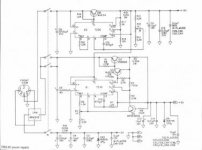
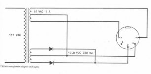
I've attached the schematic for the Keyboard (also EI) Power Supply, also the voltage regulators.

The common items that connect to all Power Supply Voltages is the System RAM (Z13 thru Z20).
You might want to remove the RAM and see if the Power Supplies act normal. That would be a
good starting point.

Remember that the +11.9 needs to be functional first and set to 11.9, then the +5.0 VDC supply functional
and set for 5.0 VDC. The -5 VDC isn't adjustable. The Voltage across C8 (2200 MFD - in +12 PS) should have
23.6 volts across it. The Voltage across C9 (10,000 MFD - in +5 PS) should have 10.6 across it. The Voltage
across C1 (220 MFD - in -5.1 PS) should be slightly above -5.x VDC, as the 5.1 V Zener will drop voltage across R19
to maintain close to -5.1 VDC. The RAM needs all these Voltages.

You might power on the Keyboard and check for some/all HOT RAM IC's.

Larry

17.jpg 16.jpg
 
Last edited:
Thanks Larry. A different Voltmeter seemed to correct the strange voltage issues. I am grounding to capacitor C9.

Pin 3 of Z2 and R18 both show a proper 11.9V. So far so good.

However, pin 3 of Z1 and R4 show 0.85V (these should be 5V according to the service manual). Adjusting R5 results in little to no change in the 5V supply - shows 0.85V.

EDIT: Voltage across C8 is 23.8 and Voltage across C9 is 12.6 (a bit high from the book's 10.6) . (Mistakenly noted Voltage across C8 was about 1V which is incorrect)

Pulled RAM and restested with same results.

Issue appears to be with the 5V supply.
 
Last edited:
Problem is most likely an open MJE34 Q6. Collector has the 12V, you say emitter is 1V on C8, base should be higher like at 1.4 to 1.6V trying to conduct current thru the MJE. Does your meter
have a diode check? No power to unit and give a few minutes to discharge then positive on base, then negative on emitter or collector should both give a junction of .6V. Looks like it has the standard ECB pin layout
so collector is center lead.

Larry G - the other Larry :)
 
Thank you Larry. I corrected my post above to properly show the voltages across C8 and C9 (23.8 and 12.7 respectively). The latter seems a bit high - diagram says 10.6. I apologize for my error.

I do not have a diode check capability. The SAMS manual says if 5V is missing to check voltages and components associated with transistors Q4, Q3 and Q5. I am not sure how to do so as Q6 and Q3 have three leads ( B C E which is what I think you alluded to). Q4 seems to have two leads on the underside. Q5 appears to have three leads, but only one labeled with an E.

With regard to IC Z1, I checked the voltages on the pins as suggested by the SAMS manual:

pins 2, 3, 4 ~0.85V
pins 5, 6, 7 0V
pin 10 1.42V
pin 11 11.9V
pin 13 2.64V

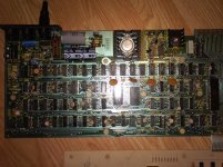
Also not sure if it makes a difference, but I should state I am working with a Level 1 system...here is a pic of the main board:

20160402_183946.jpg
 
UPDATE TO ABOVE...

Tried to test the voltages on Q6 and Q3 transistors while powered ON:

Q6
+ to B ,- to E voltage shows -0.56V
+ to B, - to C voltage shows 11.38V

Q3
+ to B, - to E voltage shows 0.55V
+ to B, - to C voltage shows -10.8V
 
If I'm looking at the right schematic, The voltage across C9 is unregulated so will vary depending on your line voltage. Z1 pin 6 being 0V is a problem. It is a fixed reference generated by Z1 which I'm guessing should be like 9V. The reference is then set on the emitter of Q5 by adjusting R5. The base of Q5 is a sample of the 5V which regulates based on the reference. I would think Z1 is bad.
 
Thanks for the quick reply! That would be an easy starting point. I'll get a new IC and swap it out. Thanks so much for your guidance Larry.
 
Cary,
Before you remove Z1 (723C) it would be interesting to see what reading you have in OHMS from the +5VDC BUS to the GROUND Plane (Minus of C9).
It's possible you have something downstream on the +5VDC Bus that could be shorted, pulling the 5VDC down.

To remove Z1, re-solder each Pin of the Z1 IC with fresh solder. Then clip each leg of the IC close to the base of the IC. Then unsolder each pin with
a heated solder sucker. (I use the Radio Shack one.) Then, for the pins that don't fall out, use your cleaned soldering iron tip to quickly heat & flip each pin
sticking through the Circuit Board to loosen them up. Most can be easily removed then. Just don't stay on each solder pad very long, so you don't
lift any solder pads.

Good Luck.

Larry
 
Hi Larry,

Just got up and read your reply. Unfortunately I removed Z1 late last night and dropped in a socket while I await the replacement IC.

Thanks for the advice on the IC removal. That's exactly the technique I use and have found it to work very well. Great advice!

If the replacement IC does not solve the problem, I will give your suggestion a try next. I should have the IC by Friday, so will report back then.

Cary
 
Like ldkraemer is saying, it's good practice to check for shorts downstream BEFORE you fire up the power supply with the new IC.
You can make his suggested checks while waiting for the chip since it might mean additional parts to order. He might be more familiar on Tandy.
I'm just working on general theory.

Larry G
 
It does sound like the chip has failed.
your symptoms and readings remind me of a Model 1 i had to repair last year...

checking for shorts on the voltage supply rails is always good practice before fitting the new chip.

:)
 
The Vref (Pin 6) of Z1 (+5.0 VDC Regulator) should have the following VDC:

LM723
Reference Voltage 6.95=Min 7.15=Typical 7.35=Max

LM273C
Reference Voltage 6.80=Min 7.15=Typical 7.5=Max


The internal workings of the 14 Pin LM723C can be explained by dividing it into two blocks, the reference voltage generator and the error amplifier.
In the reference voltage generator, a zener diode is being compelled to operate at fixed point (so that zener output voltage is a fixed voltage)
by a constant current Source which comes along with an amplifier to generate a constant voltage of 7.15V at the Vref pin of the IC.

As for the error amplifier section, it consists of an error amplifier, a series pass transistor Q1 and a current limiting transistor. The error amplifier
can be used to compare the output voltage applied at Inverting input terminal through a feedback to the reference voltage Vref applied at the
Non-Inverting input terminal.These connections are not provided internally and so has to be externally provided in accordance with the required
output voltage. The conduction of the transistor Q1 is controlled by the error signal. It is this transistor that controls the output voltage.

Non Inverting Input
This is the non inverting input of the error amplifier whose output is connected to the series pass transistor. We usually give reference voltage
or a portion of it to the non inverting input.

Inverting Input
This is the inverting input of the error amplifier whose output is connected to the series pass transistor. We usually give output voltage or a portion
of it to the inverting input. This makes the output voltage constant.

Vref
It is the reference voltage output of the IC. It is the output of voltage reference amplifier. Its output voltage is about 7.15V.

Vout
It is the output terminal of the IC. Usually output voltage ranges from 2 to 37V. This pin can provide up to 150mA current.

Current Limit
It is the base input of the current limiter transistor. This pin is used for current limiting or current fold back applications.

Current Sense
This is the emitter of current limiting transistor. This terminal is used with current limiting and current fold-back applications.

Vc
This is the collector input of the series pass transistor. It is usually directly connected to the positive supply voltage if an external transistor is not used.
Freq. Comp

Frequency Compensation
This pin is used to connect a capacitor which bypasses high frequency noises. It is the output of error amplifier. The capacitor is connected between this
pin and inverting input of the error amplifier. The prescribed value of this capacitor varies for different types of regulators. Please refer the data sheet for that.

Vz
It is the anode of the zener diode whose cathode connected to the output terminal. It is usually used for making negative regulators.
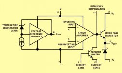


723-Voltage-Regulator-Internal-Block-Diagram1.jpg


Larry

REF: https://electrosome.com/723-voltage-regulator/
 
Last edited:
Cary,
I've OCR'd the Troubleshooting section in the SAM's Document for the Model 1, ordered it logically, and
added a few comments to make troubleshooting an orderly process.

POWER SUPPLY TROUBLESHOOTING

Computer is dead. Disconnect the Power Supply (PT1) from the CPU Board. Check for 18.5 VAC
between pin 1 and pin 3 of Connector J1A and 23.6 VDC between pin 4 (-) and pin 2 (+) of Connector J1A.
If the voltages are missing, check the cable and connections at Connector J1A and check for open AC
power cord. If the correct voltages are present, reconnect the Power Supply to the CPU Board and turn
On the Computer. Check for 11.9V at pin 3 of Regulator IC (Z2), 5.0V at pin 3 of Regulator IC (Z1),
and -5.0 VDV at the anode of Zener Diode CR2. If all the voltages are missing, check the Power
Switch (S1).

Start by verifying the 11.9 VDC, then 5.0 VDC, then the -5 VDC, because the +5 VDC Circuit requires
11.9 VDC.

If the 11.9V is missing, check the voltages and components associated with Regulator Output Transistor (Q6)
and pins 2 thru 7, 10, 11, and 13 of IC Z2. Pin 6 (Vref) should be 7.15 VDC. If the 11.9V is incorrect, check
the adjustment of the 12V Adjust Control (R10).

If 5.0V is missing, check for 10.6 VDC across 10,000 MFD Cap C9. This voltage is generated by Bridge Rectfier
CR8. Also check the voltages and components associated with Regulator Output Transistor (Q4)
(Tandy schematic shows it incorrectly as Q2), Regulator Drive Transistor (Q3), Error Amp Transistor (Q5)
and pins 2 thru 7, 10, 11, and 13 of IC Z1. Pin 6 (Vref) should be 7.15 VDC. If the 5.0V is incorrect,
check the adjustment of the 5V Adjust Control (R5).
refer to "Miscellaneous Adjustments"

If the -5.0V is missing, check Resistor (R19), Zener Diode CR2, and check for possible short to ground.


Larry
 

Attachments

  • Model1_Troubleshooting.txt
    9.6 KB · Views: 1
Last edited:
This is a great guide and starting point for those with a dead computer. Thank you for taking the time to do this Larry.

Should have a replacement 1723 in the next two days.
 
It worked! Dropped the new 723 IC in and adjusted voltages to spec without a problem.

DSC_5608.jpgDSC_5602.jpg


Thanks to everyone for your help with this. Much appreciated!

Cary
 
Cheers, Larry. Nice to see another MI brought back to life with help from the community.
 
Back
Top