• Please review our updated Terms and Rules here

More storage treasure: KDJ11-D/S (PDP11/53?) in H9275A cage with analogue, async, SCSI, ether

I'm thinking 00000040 is the bad address, not 17604666. Not near a manual right now to verify error message format though...

Update:
Yeah, OK. Checked the manual. The 17604666 is the location of the instruction that failed, so not really interesting. The 00000040/125256 <> 125252 shows:

RAM address/data read <> expected value
 
Last edited:
Ah that makes more sense - and ties in with setting it to 0.5MB being the same...

So - find RAM bit 2 in the first 0.5MB bank of ram...
 
The code at 17604666 seems like it's the RAM test code, in ROM:

Code:
17604660/020102 cmp r1, r2
17604662/001402 beq .+2
17604664/004714 jsr pc, (r4)
17604666/104124 emt 124
17604670/010320 mov r3, (r0)+
17604672/105700 tstb r0
17604674/001370 bne .-16
17604676/104027 emt 027

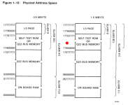
Confirmed by manual p1-23:

1710524473226.png

Next: hunting the RAM chips.

1710526196097.png
 
Last edited:
Ah it's an 11/53 specific feature having the self test ROM up at that address - maybe in the 11/93 as well, hence the confusion over the address just under the I/O space...

If you can carefully scope the pin 2 on the RAM chips and just do a short loop of a mov 40,0 and mov40,4, br -7 then one ram chip in the first bank should show a different pattern to the others (there will be 3 chips in all on D2) - you need to disable the CACHE with the cache control register - it may be disabled in any case due to the ram test, but needs checking. The correct ram chip should show more activity on the /RAS and /CAS lines than the other two

Halt on Break is almost always disabled on production systems as it halts the CPU if the console is turned off... Handy for testing though if you haven't got a halt switch
 
The patient is on the bench next to the scope, ODT has been administered, and am trying to run variants of this:

Code:
00000000/012700     mov #xx, r0
00000002/000004     xx
00000004/012701     mov #dd, r1
00000006/000040     dd
00000010/010011 q:  mov r0, (r1)
00000012/000776     br q

Got a few scope traces but I didn't immediately make sense of what I was looking at. I'm reading DCJ11 Microprocessor User Guide (appendix D) to try to understand the bus timing: I think the mov r0, (r1) is 3 and the br is 4, I'd expect three /ALE on the CPU (with addresses 10, 40, 12) and perhaps some kind of recognisable pattern on AIO3 (maybe 1, 0, 1) and 12 ticks on CLK.

Jonathan.
 
Last edited:
Your writing the same value over and over - try toggling bit 2 and looking for the DRAM with the toggle pattern...
 
I think you're going about it the hard way. The goal is to find the bad RAM chip, is it not?

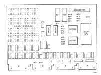
We know it's in the lowest 512KB, and that puts it in the bottom two rows of chips
M7554 Layout.png
The optional chips for a 1.5MB card are shown dotted...

Now, we know it's bit 2 of the low byte from the memory self-test output (00000040/125256 <> 125252)
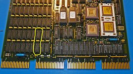
But which is bit 2? It's one of the chips circled in yellow:
M7554 RAM.jpg

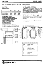
How do we know that? Well, we know the pinout of the ROM chips and a continuity tester shows D2 (pin 13) of the left-hand ROM (262E5) connects to the Q output (pin 14) of the chip in the bottom row, while D2 of the right-hand ROM (261E5) connects to Q2 of the one in the second row. Now we just have to figure out which is the low byte. That is left as an exercise to the reader, but someone should know based on the ROMs(*) (or: swap them both out, or: try one and if that doesn't fix the problem, try the other - but on my board at least, the pins are bent over on the back side of the board which will make it harder to save the chips when removing them). No oscilloscope needed. 🙃

(*) OK, according to this page: https://www.pcjs.org/machines/dec/roms/assorted/
262E5 is the low byte. That's the one on the left, so the bottom row of RAM chips should be the low byte.
 
Last edited:
Well, I looked for documentation but didn't find anything that explained it as well as you have! Thank you, it's really helpful.

Do you know how to run a RAM test which doesn't stop at first fault? It would be good to get a feel for how many chips are faulty.

I was considering swapping bank 0 bit 2 chip for bank 2 bit 2 chip, to put the fault in the optional space: changing W25 should then produce working 512Kbyte system.

Sadly this morning I'm seeing

RAM VPC=024454 PA=17604454 00000000/177576 <> 177776

1-111-111-101-111-110 found
1-111-111-111-111-110 wanted

Jonathan.
 
Last edited:
If the fault is in the bottom 64KB ram, you're going to have trouble running the proper diagnostics in XXDP, like VMSA?? for the RAM - so best to snip out the faulty chip(s) and put a socket in with new chips - this is the least risk to the board itself and hopefully there are only a couple of faulty chips - but this is the issue with boards like the 11/53 with so much on one board...
 
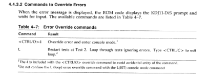
I did find that: it appears to loop the tests but without output. I ran it, interrupt with CTRL-C, says it ran the tests 257 times with 257 fails.

Code:
KDJ11-D/S   4.55                                                             
Error, see troubleshooting section in Owner's manual for assistance
RAM    VPC=024454  PA=17604454  00000000/177576 <> 177776

KDJ11-D/S> L


257/257

ODT is suggesting there's trouble everywhere. I'm wondering whether it's could conceivably be something like the 73LS240 buffers or indeed anything else. Do people find the RAM chips go wrong like this, in general terms?

The date codes suggest this machine is only 30 years old.

# bank 0
Code:
@0/000200 0
@0/000200 177777
@0/177776 1
@0/000200
@?
@1777776/000201 0
@1777776/000201 177777
@1777776/177777 0
@1777776/000201

# bank 1
Code:
@2000000/000200 0
@2000000/000200 177777
@2000000/177777 0
@2000000/000200
@?
@3777776/177777 0
@3777776/000200 177777
@3777776/177777 0
@3777776/000200
# bank 2
Code:
@4000000/010000 0
@4000000/010000 177777
@4000000/177777 0
@4000000/010000
@?
@5777776/010000 0
@5777776/010000 177777
@5777776/177777 0
@5777776/010000

I'm still thinking about how to run some more extensive tests to get an idea of how many replacement RAM chips I might need.

Jonathan.
 
Hmm - Odd - but like you say, 30 years old.. We also do not know how well (badly) it has been handled or stored, I would start with bank 0 and see if you can get 512KB working, then you can jumper it as a 512KB board and run the XXDP diagnostics... I take it you have a solid +5V supply on short cables to the backplane?
 
The board looks exceptionally clean, not even fluffballs which makes me think it was possibly never used. I've had for about 20 years, always in good clean dry storage. I'm going to do some double-checking of power supplies and so on and very close visual inspection. I really don't want to take a soldering iron to it unless absolutely necessary, but if so, perhaps putting sockets on all the RAM.

Jonathan.
 
ODT is suggesting there's trouble everywhere. I'm wondering whether it's could conceivably be something like the 73LS240 buffers or indeed anything else. Do people find the RAM chips go wrong like this, in general terms?
It could be something other than the RAM chips, but the 240s are not in the path between the RAM and the CPU. In fact, there's a direct connection between the data outs (of both the RAM and ROM chips) and the CPU.

From your ODT probing, it appears that there are 4 bad RAM chips:
- Bank 0 bit 0: stuck at 0
- Bank 0 bit 7: stuck at 1
- Bank 1 bit 7: stuck at 1
- Bank 2 bit 12: stuck at 1

And Bank 0 bit 2 has miraculously healed itself.
That all seems very strange. I'm starting to suspect something else, like maybe bad solder joints? Or maybe the refresh circuitry, but then I'd expect more random errors... Any kind of a bus conflict would likely show bits stuck (or randomly) at 0, not 1 - logic low generally wins the battle between 1 and 0 (and the data lines are not inverted). But stuck at 1 is a common failure mode for dynamic RAM chips...

I'm still thinking about how to run some more extensive tests to get an idea of how many replacement RAM chips I might need.
Yeah, you're going to need some reliable memory to run out of. We know the ROMs work OK, so creating new diagnostic ROMs (and staying in the registers) is an option. But not a very practical one. The other option is to add a memory board like an M8059 on the Qbus and run the code from there...
 
If the fault is in the bottom 64KB ram, you're going to have trouble running the proper diagnostics in XXDP, like VMSA?? for the RAM - so best to snip out the faulty chip(s) and put a socket in with new chips - this is the least risk to the board itself and hopefully there are only a couple of faulty chips - but this is the issue with boards like the 11/53 with so much on one board...
FYI I have my home grown memory diagnostic I use for checking my 11/34 and 11/44 systems.
Requires only a bare minimum of the first 8KB to be working, and will test a fully loaded 18b or 22b memory configuration.
It is not system specific, and will run on anything from an 11/03-04-05 thru an 11/70-84-94.
It is MEMX.* available here: https://ak6dn.github.io/PDP-11/DIAGNOSTICS/ as .BIN and .LST and .MAC files as well.
Under here: https://ak6dn.github.io/PDP-11/TU58/11XX_9.DSK is an XXDP bootable TU58 image with MEMX.BIN on it.
My bad. Correction: it DOES require a PDP11 with memory management, so 11/03-04-05-15-20 are not supported. 16KB is the minimum required memory.
Memory management is used to relocate the program image to more easily test the low 8KB memory as well as all the memory above the 56KB boundary.
 
Back
Top