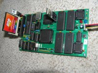
I think PGA is preferred because it is easier to assemble by hobbyists and can be removed for troubleshooting or salvaged for another project. 68020 and 68030 epoxy PGA are fairly inexpensive.
That is certainly true. I understand the motivation to use PGA, which can be reused, especially since it is very expensive, especially for 68060.
As for design problems, I have the impression that wiring routing is difficult with PGA.
In my 68SEC000 project, I made it possible to use a flash ROM with a PLCC-PGA conversion socket, but I felt that the wiring in this part was difficult to do even with 4 layers (especially when the priority is to make use of the power plane).
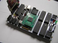
On the other hand, the layout of components for efficient routing and FPGA pin assignments were very careful because the space between pins is narrow when using a flat package.
The FPGA pin assignments are not completely free (there are recommended pin assignments for some applications), so I had to consider that as a constraint, and I felt that this was not a problem that could be solved just by using FPGAs.
In fact, there was a time before I started this project when I wanted to somehow do it with DIPs and PGAs forms, but after doing a small-scale flat package implementation, I found that handling the stencil, handling the solder reflow oven, and hand solder rework techniques (see the YouTube demonstration of our predecessors), I found that it was not that difficult, so I switched to a policy of using flat packages across the board.
Video of hand solder correction:.
This is not the video I saw, but it looked almost identical to this one. It looks like you just squeeze out the flux in a syringe, apply it (very roughly), and trace it with a soldering iron.
This video seems to be an advertisement for this flux paste, but I think it should be fine as long as the flux is not of poor quality (mine is not this flux paste).
The points are:
* As shown in the video, apply as much as you think is too much.
* Trace quickly.
* Use less solder. If you use too much, it will accumulate at the end of the pins (even in this video, there is a small amount of solder on the remaining two pins.)
* The tip of the soldering iron should be flat.

") ).
).