nikola-wan
Veteran Member
What other options do you think you have? There is another sticker inside the computer - on my 4054 monitor that lists options installed at the factory.
| VCF West | Aug 01 - 02 2025, | CHM, Mountain View, CA |
| VCF Midwest | Sep 13 - 14 2025, | Schaumburg, IL |
| VCF Montreal | Jan 24 - 25, 2026, | RMC Saint Jean, Montreal, Canada |
| VCF SoCal | Feb 14 - 15, 2026, | Hotel Fera, Orange CA |
| VCF Southwest | May 29 - 31, 2026, | Westin Dallas Fort Worth Airport |
| VCF Southeast | June, 2026 | Atlanta, GA |
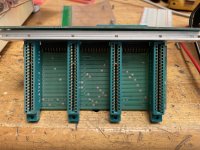
I think we can try to diagnose whether backpack slots 51, 61 or 71 work.I reached out to Jos to get a diagnostic pack, I just hope it works given my lack of success with any of those slots in the Backpack.
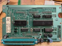
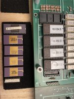
I burned new EPROMs to deal with the ROM rot, and those were the v5.1 images that Jos shared somewhere.
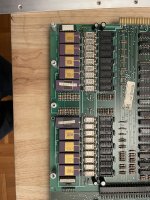
Looking at the pics from the last time I had the board out (to swap the ROMs) it does look like I only have 32k installed.
I'll start looking for replacements, but I think I'm going to wait to poke at this any more until I get that diagnostic pack.
oh, and I did hear back from Tek museum, they're going to look into those microfiche scans tomorrow - thanks for the suggestion!

The DRP you'll receive is tested, so if it does not work at your end you'll have to debug the 4052 end.I reached out to Jos to get a diagnostic pack, I just hope it works given my lack of success with any of those slots in the Backpack.
Important : which images exactly ? I posted 2 versions, the original ones ( can be found on bitsavers ) and a transposed one, intended for wsi57c49 EPROMS ( slightly dirrefent pinout) . You are using MCM68766, hence you will need the original set.I burned new EPROMs to deal with the ROM rot, and those were the v5.1 images that Jos shared somewhere.
Indeed. Just add 4116's when all the rest ist functional !Looking at the pics from the last time I had the board out (to swap the ROMs) it does look like I only have 32k installed.
Important : which images exactly ? I posted 2 versions, the original ones ( can be found on bitsavers ) and a transposed one, intended for wsi57c49 EPROMS ( slightly dirrefent pinout) . You are using MCM68766, hence you will need the original set.
Jos - Oh yeah, I didn't mean the DRP was going to be bad, I'm just worried that if I've got bad slots, I can't use it.The DRP you'll receive is tested, so if it does not work at your end you'll have to debug the 4052 end.
A command to try with the 4052 File Manager is:
CALL"SETTIM","9-AUG-23 9:30"
or
CALL "TIME",A$
I'm not sure where you are measuring the backpack bankswitch signals.Jos - Oh yeah, I didn't mean the DRP was going to be bad, I'm just worried that if I've got bad slots, I can't use it.
Monty - the file manager is another ROM Pack, ya? Calling those with my machine in it's current state gives the same "CALL NAME INVALID" error.
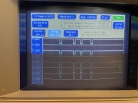
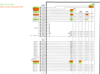
I did some more shots with the logic analyzer (an HP 16500B). Here's power-on. It takes about a half a second to see data on the bank switch lines, but it doesn't look like I'd expect, in terms of them all being in sync (the ones that work). It looks the same at higher sample rates.
The inactive lines also don't correlate with one of the 74138 select lines being bad.
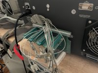
I'm worried that without a working backpack, I'm not going to be able to check the RAM. I'm also not sure what to suspect next, besides the MC6821PIA. I do have one I pulled out of a Tektronix 7D01 (in all it's beautiful purple ceramic glory)... worth swapping it out?


right?during power up you should see all the combinations of bankswitch numbers plus the additional combinations for slots 61 and 71.