• Please review our updated Terms and Rules here

MFM decoder for RL02 = up and running but sector/header format unclear and ...

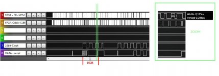
Would it be easier to prototype with ST-506 so you didn't have to deal with the 4.1 clock or explicit data format?. You could concentrate on MFM encoding/decoding @ 5MHz and let the controller write a low level format to test with. Then once that works, move to 4.1 MHz and write a utility to 'low-level' format your SD cards. Just a suggestion :)

I think this is what he was hinting at when he last mentioned the ST506. I sense he is beyond frustration, and it is taking it's toll on him.

Despite my encouragement, I am not there and I feel he has a need for a sense of accomplishment.

It is true, this [ST506] would be easier to do than what he's trying to, but I am afraid he will lose the "mind set" it has taken to get this far by moving on to another project. The fact is that he'd still need to solve this framing issue in the ST506 too.

I have faced "burn out" myself at many times, and "therapy" projects do help. However, they have the potential to take one away from "critical mass" on the primary project. I feel if he pushes through this he will achieve the breakthrough that will make it all worthwhile.

Of course, it's just my opinion, and in the end he will make the decision. All I can do is offer support.
 
...What do you think about the following idea: Remove the EPROM 2708, E8 on a RLV11/M8013, read the contents and import the data in the FPGA world ? I think the secret is in this EPROM based on the flow chart info in the RLV-11 engineering drawings. I am thinking about this, because I got the message yesterday, that the computer museum in Munich could find RLV-11 ( M8012,M8013 ) boards....

E8 on the RLV11 is the Write Precompensation EPROM. It's used to look at the MFM bit patterns during WRITE and add or subtract time from the transitions so that the data will appear as intended on read back.

It is not used during READ when data is coming from the disk. It is only used on WRITE and effects data coming FROM the controller. So you only need to be concerned with it when the CONTROLLER is WRITING to your SD card.

See discussions concerning "Write Precompensation".
 
Hello,
if you want to go in details concerning ST506/MFM disk formating, please find attacht a MACRO-11 format program for the RD50(1) which was part of the professional 350
 

Attachments

  • RDFORM.MAC.txt
    10.1 KB · Views: 1
Hello,
I have thought about it and agree with you : "The SERVO data is not processed in the RLV at all."This meens for me and my project: Modify my MFM decoder in such a way to be able to slit out the headerinfos only , triggered by the both sync bits 47="1" in PR1 and PR2. The header info is is absolutely necessary for me, to construct a pre-formated SD card. By the way, alignment at byte boundary is not implemented, because this is implemented based on a union statement in c programming. For the outstanding MFM-encoder, I have to send only dummy data with 2 sync bits at the servo section to satisfy the logig of the RLV controller. You agree?
Anyway , this will also be a "try on error" work ... but I like it.
Additional infos:
- I will continue to work on my RL02 simulator project. You have motivated me very much here in the forum, Thanks.
- Seems to be , I will get an RLV11 controller next Week and I can continuing to work.
- I will not start the MFM/ST506 project, this is your task. But if I can help somehow, please give me a call. I like to do this.
At least a completely new idea has occurred to me . I can remember very well to the possibility to expand a Q-Bus or UNIBUS and on the other hand, nothing speaks anyway to connect the expanded Q-Bus to a FPGA environment. No MFM de/en-coding is necessary and we do not further need each other around disk concern things. In this case we only would work with data. Faking the CSR's would be very simple. Data transfer also can implemted very simple based on a dual ported RAM. I use a Altera DE1 development board and there are 68 pins available to connect a Q-BUS or UNIBUS. An effort would be necessary to convert the open collecter signals to the FPGA world. But this realy is realisable. Maybe, the DC003/Dc004/DC005 Q-BUS protocoll chip should be attached before the FPGA ?
Anyway, if you also like this idea, we should open a new discussion round ?
Best Reagrds, Reinhard
 
RL emulator?... ST506 MFM drive emulator?... QBUS option? UNIBUS?...

LOL - You are ambitious and full of good ideas!


  • Let's take the QBUS first - I have designed UNIBUS and QBUS devices, and worked with UNIBUS cards in production under license. A lot of support tools have to be made to ensure these work correctly. But perhaps the most intractable obstacle is simple cost. PCBoards cost based on the area and weight here.
This translates to a higher price to implement a solution at this level. [this problem applies even more to the UNIBUS] Then there is the added complexity, particularly in the debugging phase of the project.

It's at least an order of magnitude more resource intensive in all dimensions.
  • ST506 MFM Emulator - I have no monopoly on this idea. Frankly, I was surprised to see that one had never existed for under $2000. If it cost as much as an IDE-SATA adapter, I would own one.

I'd be happy to work on this with you. You have a similar sense of humor, and tenacity as I. But let's get your RL emulator going first, ok? Once you're done with the RL "interface" side, you'll be getting to the real work.

  • Your RL emulator does need to be able to respond to the RLV with HEADER frames. This is true. However, it has not escaped my notice that you do not need to save these. You COULD simply generate a header that should go with the SECTOR the RLV requests. In other words, it doesn't need to be "SAVED".

[Don't mistake me here - I am not advocating this approach. I merely am saying it is valid... not that it is BEST.]

  • I'm glad you can get another RLV.
Be very careful about the RLV11. Puttting it in anything other than an ABCD slot will result in physical damage to the card.


Finally, I'm very happy you are going to keep going on your RLe [RL emulator] [mind if I coin the acronym?]

I eagerly anticipate seeing the data from your next version!

Best Regards
 
Hello,
good news of me and my Project.
I did re-soldering my RLV-12 controller again and was able to bring it up and running.
I do not know the fault cause, however, it works again and this is the most important to me.
The second good add new: I did revised the design of my MFM decoder, that I am able now to
spit out the header information from the servo section. Enclosed please find the picture, which illustrates my implementation. Although it is not important in this phase yet .. but I still see not valid MFM signals in the HEADER-CRC section like 0.125uS MFM signals. This surely becomes a topic again when I start to develop the MFM-ENCODER soon.You find exact upgrade infos on my hompage
(www.pdp11gy.com) , chapter 1.7 very soon.
My last point: I have a bad feeling concerning my RLV-12 controller. In the meantime I got one
module of a RLV-11 controller, the M8013 but I still need the M8012. If somebody has an idea where I can get a M8012 module, it would be very grateful for me.
Best regards and many thanks for the cooperation, Reinhard
RL02-format.jpg
 
Good to hear from you Reinhard.

I just spent a few minutes looking over your changes.

Can you tell me where in your diagrams you are detecting the PR1 [Header Preamble] data pattern to arrive that is used to SYNC the "16Bit_synchron_counter" to?

Am I missing it?
This would be a stage where you see the previous 31 bits output from the MFM decoder equaled "0" and a "1" has just been received. This aligns the succeeding bits to 16 bit frames. From this point, the number of bits expected in the header can be counted.

When the counter is satisfied, the "Framing" detector should be forced "out of sync" again and begin looking for another Preamble. When satisfied, this will be PR2 and provides sync for the DATA frame to follow.

Another question which puzzled me before, but I didn't ask...
What is the "WordCount" at the beginning of your data columns in these diagrams?
Is this something output by your tools? It's not part of the header in any documentation I've seen.
 
Hello,
Here is the data flow description with reference to the “Zyklus_Starter“ circuit diagram which initialize all the detecting stuff.
a) The 4.1666 Mhz MFM-clock becomes started with the first MFM signal edge
b) Two counters will be started by the MFM-clock. The output signals of these counters
are “IN_PR1_L“ and „“IN_PR2_L“
c) PR1-PHASE: The “IN_PR1_L“ signal becomes active in the middle of the PR1 section. 16Bit
clock still is disabled until the PR1 sync bit is detected to restart the 16Bit counter synchronously.
d) Header-Phase , 16Bit counter is enabled now to be able to receive data via parallel strobe.
e) PR2-PHASE: “IN_PR2_L“ signal becomes active in the middle of the PR2 section and starts
following sequence: 1= disable 16Bit counter, 2= clear(preset) 16Bit counter, 3= force the
output to a “0“, 4= wait for the PR2 sync “1“ Bit, 5= restart the 16Bit counter synchronously.
f) Data section, read the data including data CRC.
In my diagram from my last post , you will find the logic-analyser signal “16Bit enable“. If this
signal is high, a data transfer is active and synchronized to 16Bit boundary.
In the Header section of the RL02 disk cartridge format appears sometimes a not valid MFM
signal which illustrates following picture. This “not valid MFM signal“ in the header section upsets
my MFM-Decoder. This is the reson why I force the output to a “0“ in the PR2 section. I still
don't know why this is so. ...?.... it will be figured out and solved in the phase designing the
MFM-Encoder !
At least, the word count value is only included for debugging purpose in my C-program.
Regards, Reinhard
 

Attachments

  • HDR-symtom.jpg
    HDR-symtom.jpg
    50.7 KB · Views: 1
I was afraid you would say that. The section "8_16_64_128_Counter_C" appears to be "counting" MFM clock pulses.

I don't think this concept will work. The "Phases" of the "zyklus_starter_V5" do approximate what is needed, but counting MFM clocks won't get you the triggers you require to frame data correctly.
It needs to examine the NRZ data for 32 bits and output a trigger whenever that data chain constitutes a "Preamble" [31 zeros followed by a "one"]

From then on, you can count to establish the ends of the HEADER and DATA if you like.
I'll look around for a description of this concept on the web when I have another minute. So far none were concise enough to be illustrative. It's commonly used in BiSYNC, SDLC, HDLC data streams to FRAME bytes correctly where long serial bit streams are handled.
 
I am afraid now that you are afraid.
I have uploaded a new and a little modified MFM_DECODER_v2 file on my homepage.

First of all, this concept works, because: A logic analyser cannot lie :))

Also, the dump routine works a littly tricky but shows me exacly, what is going on.
It is so, because the 16Bit output shift-register will be clocked continuously,
also during the 16bit-counter-disable timeframe. If the 16Bit counter gets enabled,
I will receive the last 16Bit remaing in the shift register. It is always(!):
00000000
10000000
|>------------------Sync Bit (MSB) = "one" at the end of PR1 and PR2

I am aware about the fact: "31 zeros followed by a "one" and my design takes
care about it. I do not want to justify myself further. You can assume that
my design works.

Many thanks for your offer according to other references to furthermore look
This is not necessary and I do not want to steal your time either.

I will start now designing the ENCODER. I am curious what the RLV controller
does very tensely if I send MFM encoded data.
I still don't understand...

I expect the PReamble sequence:
00000000
00000000
00000000
00000001
Where am I going wrong?

Good luck with what you decide. I consider myself dismissed.
 
Last edited:
It's related to LSB and MSB and believe it, I also failed to understand this first time.
For example: to receive the pattern 11000101 , you have to write it beginning with
LSB: 10100011 ... Reading: LSB comes first in .. result: 11000101. PDP-11 is a
byte boundary orientated little-endian architecture ( in contrast for example the MC68000)
For you, also good luck and all best with your hobby.
 
Back
Top