• Please review our updated Terms and Rules here
  • From now on we will require that a prefix is set for any items in the sales area. We have created regions and locations for this. We also require that you select a delivery option before posting your listing. This will hopefully help us streamline the things that get listed for sales here and help local people better advertise their items, especially for local only sales. New sales rules are also coming, so stay tuned.

WTB: Logic Analyzer ~25 MHz for 8 bit debug

atod

Experienced Member
Joined
Oct 14, 2010
Messages
303
Location
New York, NY
Does anyone have or know of a cheap LA? I'm trying to debug an ADDS terminal and Northstar S-100 bus FDC. A LA would be very useful. Most of the ones on Ebay are missing probes and the ones that have them are very pricey.

Thanks!
 
If you don't need a lot of channels/fast sampling, you can use the parallel port:

http://www.xs4all.nl/~jwasys/old/diy2.html

There's also a good parallel one at Berlios.de:

http://developer.berlios.de/projects/tfla-01/

Not 25MHz by any means, but it's free.

In general, the inexpensive ones, including the FPGA one given above, do have severe limitiations when compared with standalone analyzers. For example, good analyzers have glitch detectors and allow for a wide variety of displays.

I suspect that the probes for the analyzers being sold on eBay have wound up in some copper scrapper's bin...
 
Thanks for the options folks! I'll probably try out the parallel port one and if that doesn't work, purchase the $50 USB version. I do get a little worried about hooking up DUT voltage directly to the parallel. What if I bump a probe into a high voltage line...
 
I looked at the schematics and the later Berlios distro had something to isolate parallel port from the bus. It also has what appears to the circuitry to connect to a serial line. Pretty neat.
 
There is a local (40 miles away) buisness that scraps used electronics. I called them an asked if they ever got used test equipment to scrap. They did and what was I looking for, so I got an HP 1650a logic analyzer with probes and manuals for $50. I also got an HP digitizing o-scope for around the same price. Both units work great. Just a thought..
Kipp
 
There is a local (40 miles away) buisness that scraps used electronics. I called them an asked if they ever got used test equipment to scrap.

Great idea. Unfortunately not all scrapping outfits do this. Here on Long Island I tried a couple of times but they do not even respond to email and voicemail. :(
 
I just tried the one near me in Hudson NH, nothing.

I reviewed the schematics for some of the open source LAs which pretty much use the parallel port with signal isolation to the port:
digitrac_scheme_active.png

tfla.jpg


I would have expected them to use the IRQ when Pin 10 (nAck) transitions for higher capture rate. It doesn't look like they do this as that pin is not connected. It's simply the 8 IOs that are sampled. Must be a polling loop. Wonder how efficient that is and the rate that port can be polled on 1.8 GHz laptop.

One page says 1 million samples / sec, which is about 1 MHz.

For $50, this up to 100 MHz / 32 channel home LA board seems a pretty good deal. It has internal and external clock IO. It even has serial, SPI and I2C protocol analysis.
http://gadgetforge.gadgetfactory.net/gf/project/butterflylogic/
 
For $50, this up to 100 MHz / 32 channel home LA board seems a pretty good deal. It has internal and external clock IO. It even has serial, SPI and I2C protocol analysis.
http://gadgetforge.gadgetfactory.net/gf/project/butterflylogic/

I've used mine to capture some low bit rate serial traffic from a car head unit to DSP. It worked great. Be warned it mailed from China and took about 4 weeks to get to Atlanta. Not sure why. It's basically a FPGA, PIC, and buffer on a board with all the software (host, PIC firmware, and HDL) opensource. So you could use it for more than just a logic analyzer. Only 16 of the lines are buffered. The other 16 are run to through hole pads but not stuffed and are LVCMOS but with internal pull up/down control to 3.3/0. Be sure to order the breakout clip cable if you don't have clips already.
 
I've used mine to capture some low bit rate serial traffic from a car head unit to DSP. It worked great. Be warned it mailed from China and took about 4 weeks to get to Atlanta. Not sure why. It's basically a FPGA, PIC, and buffer on a board with all the software (host, PIC firmware, and HDL) opensource. So you could use it for more than just a logic analyzer. Only 16 of the lines are buffered. The other 16 are run to through hole pads but not stuffed and are LVCMOS but with internal pull up/down control to 3.3/0. Be sure to order the breakout clip cable if you don't have clips already.

Was the serial capability a separate adapter? The page indicated there was a "legacy serial header". I'm assuming I need an adapter to do serial. I bet the adapter converts 12V logic levels to 3V. If the other 16 lines are not buffered what are they used for?

Thanks
 
Actually, there are a bunch of RS232 -> TTL level convertors on Ebay for about $3.00. They cover GND, RXD/TXD, RTS/CTS. Pretty cool! Thats probably cheaper then procuring the MAX232 ASIC itself.
 
If CPU's not doing anything else, polling can be faster than using interrupts.

The range of possibilities, given cheap microcontrollers, is pretty broad. Here's one for under $10:

http://www.tedrossin.0sites.net/Electronics/Pic/Pic.html#LogicAnalyzer

SparkFun has one for $149 that claims 25Ms/sec.

I looked at those schematics and the Fabulous Logic Analyzer has a 10 pin header for the analyzer probes. I'm wondering, if I were to have like a 6 foot ribbon to a set of probe clip breakout box, wouldn't the ribbon need to be 20+ pins? Every other pin would go to ground? I.e. to prevent interference?

Thanks
 
You've just hit on why real logic analyzer probes are so expensive when you do find them for sale. While it might work for 1MHz signals, I sure wouldn't want to use 6' of unterminated ribbon cable (or cotton-covered push-back wire for that matter) on a probe. The combination of no termination and lead length could cause enough ringing and reflection to affect the circuit that I'm probing!

It's true that there are printer cables longer than that, but they have a defined handshake sequence and don't usually run at 1MHz.

I'd probably move the receiver circuit out to the end, say with no more than about 8" of lead per probe and use differential twisted pair between the "head" and a transmitter at the PC end.

Or just use one of the uC designs and position it close to the far end.
 
Was the serial capability a separate adapter? The page indicated there was a "legacy serial header". I'm assuming I need an adapter to do serial. I bet the adapter converts 12V logic levels to 3V. If the other 16 lines are not buffered what are they used for?

Thanks

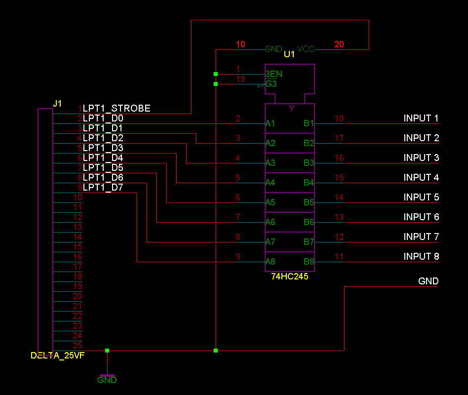
I just used 4 lines on the 16 buffered inputs to capture clock, data, reset, and bus-on signals in parallel. The other 16 lines as well as the other headers are there for expansion.

- 1x18 pin right angle header with capture lines 0-15 from the '245 buffer & 2 grounds. Any of which or a combination can also be used for trigger on a variety of conditions.
- 1x18 unstuffed header for capture lines 16-31 at unprotected LVCMOS levels
- 2 separate unstuffed 1x4 headers with 5V, 3.3V, 2.5V, & GND
- 1x4 unstuffed header with RS-232 TX & RX from the PIC, USB +5V supply, and GND
- 1X5 unstuffed header with GPIO P6C & P6D from PIC, 5V, 3.3V and GND
- 2x2 unstuffed header with separate CLKI, CLKO, TRGI, TRGO signals (all wired to PIOs on FPGA - as outputs for external logic)
- 1x8 unstuffed header with SPI clock, slave in, slave out, slave select, and 3.3V, one GPIO from PIC and GND x2.
- All headers use standard 100 mil spacing
- There are update and reset switches present
- There are power, usb activity, arm and trigger LEDs present
- The FPGA has an external 50 MHz XO, the PIC an external 16 MHz crystal. I presume both are bumped significantly with internal PLLs
- PIC is a 16F2450 in a SOIC-16 package
- FPGA is a Xilinx Spartan-3E (S250) in a TQFP-100 package
- Buffer is a Phillips LCX16245G in a TSSOP-48 package
- Micro-USB connector - cable not included
 
Last edited:
I looked at those schematics and the Fabulous Logic Analyzer has a 10 pin header for the analyzer probes. I'm wondering, if I were to have like a 6 foot ribbon to a set of probe clip breakout box, wouldn't the ribbon need to be 20+ pins? Every other pin would go to ground? I.e. to prevent interference?
6 foot? jeez. With a ribbon cable I would stick too 6-12 inches. What Chuck said about low impedance probes being expensive for a reason.

Use one of the USB ones and place it near what you are probing and then carry the capture dump via USB at high speed over whatever distance you need.
 
Back
Top