• Please review our updated Terms and Rules here

Repairing TRS-80 Model III video circuit + identifying diode

Scott Kevill

Experienced Member
Joined
Aug 22, 2011
Messages
60
Location
Perth, Australia
I've rescued a TRS-80 Model III that has been in someone's shed for at least the last 20 years. Aside from the four mice skeletons I found inside it, the video has some issues:
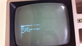
m3_vid_problems.jpg

I haven't done any work with CRTs before, but this looked like a problem with the vertical deflection. The text should be at the top of the screen but instead starts at the centre. The actual text was flickering fairly rapidly, and of course the mushed up dots in the centre shouldn't be there. The intensity of those match the text below them.

So I looked over the schematic from the Model III Technical Reference Manual (in particular the "TOP VERTICAL OUTPUT" section) and the voltages were quite a bit different. The supply voltages were fine though.
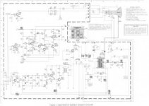
m3_vid_schem.jpg

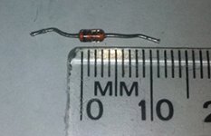
Now the interesting part was the voltage drop across the diode CR609 was 0.1V. Aren't diodes supposed to have a voltage drop of at least 0.7V? CR610 was listed as an identical stock number and it had a voltage drop of 1.6V (if I remember correctly) which was a red flag. Unfortunately the replacement part list doesn't specify any details about the diode other than it is "silicon". I de-soldered it so that I could read any info from the diode itself, and it has A24 on one side, and 031 on the other side. A little hard to see from the photos, but you can make it out:

m3_vid_diode_a24.jpgm3_vid_diode_031.jpgm3_vid_diode_size.jpg

I couldn't find any useful information with Google from this info. Any ideas? And am I on the right track?
 
I always like to start these projects with a recap of all the electrolytic capacitors first and foremost as it usually saves time and they are the most failure prone parts in old electronics.. Have you done this yet?
 
I haven't replaced any capacitors yet. I was hoping to keep the board changes to a minimum, and the diode voltage differences seemed like a glaring red flag.
 
Did you try adjusting R617 Vertical size? Sorry if this seems like an obvious question. At least the diodes are not Zener. Might be able to get by with replacing with 1N4002 100v 1amp silicon diode.
 
Schematic is a little small to read! and I can't seem to easily find another copy, it definitely looks like the top transistor isn't being driven properly or for some reason isn't able to do it's job, but without the schematic I couldn't hazard a guess. any chance of posting a link?
 
Did you try adjusting R617 Vertical size? Sorry if this seems like an obvious question. At least the diodes are not Zener. Might be able to get by with replacing with 1N4002 100v 1amp silicon diode.

I did try all those adjustments first, but they didn't make much difference. The character size does look correct, so I don't think it would be related to Vertical Size. Even Vertical Position wouldn't really explain it.

Schematic is a little small to read! and I can't seem to easily find another copy, it definitely looks like the top transistor isn't being driven properly or for some reason isn't able to do it's job, but without the schematic I couldn't hazard a guess. any chance of posting a link?

Ahh! Sorry, I didn't realise this forum resized attachments. Yes, that schematic is way too small! Here are the images as originally intended:
 
IMO I don't think it is the CRT. What size transistor is Q606? Could you post a pic of it. Almost makes me want to get my Model III and take a look at mine...
 
The diode is good if, when you use an ohmmeter, it shows that it blocks current flow in one direction.

Funny; the first thing I would have checked is C610. A bad unit there would cause the low voltage reading.
 
Horrible circuit diagram, looks like it's been drawn by a draughtsman, not an engineer, very little flow in the less obvious bits of the circuit.

I agree with Chuck about C610, but... I would guess at C605 being short, has pulled the "dead" end of the vertical deflection up to 18 V. That gives the output transistor nowhere to go. I'd replace c605, c606, and 610 while you have the board out. & go to the next voltage rating up as it will probably still be smaller than the original., and more reliable.

p.s. I reckon C605 is a snubber for the excess yoke current, so has probably had a hard life.
 
Thanks, I guess it makes far more sense that it would be the capacitor than the diode. Especially now that I've read more about the reliability of electrolytics.

Took some more photos of the board:

C610 (0.68uf, 80V) is the small axial cap next to the space where I removed CR609. C605 and C606 (220uf, 15V) are the other two larger blue radial caps.

C610 looks like it is bulging at the -ve end.

Local stores have 220uf electrolytics in 16V and 25V, but no such luck for the 0.68uf at high enough voltage rating. Can I replace C610 with a non-polarised equivalent MKT or greencap polyester?
 
That should work okay, but use a 100WV one.

What's the cap with the brown gunk all over it in the last photo?

Also check Q606. PNP power transistors are generally inferior in terms of reliability when compared with the NPN variety.
 
The gunked-up cap is C605.

How do I check Q606? Just the voltage measurements at each point? Does it make sense to do this only after replacing the caps?
 
Replaced C605, C606, and C610. No change, other than perhaps slightly cleaner formation of characters (though I could be imagining that). Original deflection problem is still there.
 
The gunked-up cap is C605.

How do I check Q606? Just the voltage measurements at each point? Does it make sense to do this only after replacing the caps?

I assume that you've checked your diode for diode-like behavior.

For transistors, the best way is to remove the device and check it out of circuit. See testing tip here.. BJTs mostly fail short between two terminals; normally, emitter-to-base and base-to-collector junctions should behave as diodes.
 
I assume that you've checked your diode for diode-like behavior.

Yes, with the ohmmeter it was open in one direction, and I think 865K in the other direction.

For transistors, the best way is to remove the device and check it out of circuit. See testing tip here.. BJTs mostly fail short between two terminals; normally, emitter-to-base and base-to-collector junctions should behave as diodes.

Thanks, I'll try to do some more tests tonight.
 
that's a cooky set of voltages! I'll have a further look tomorrow evening (for me) see if I can make any sense. They were taken with no video signal going in weren't they? I'll tell you what does look disturbing, the voltage across R626 in spite of both the output transistors being turned off. Either they're funny readings or that's a very open/hot resistor.
 
Last edited:
that's a cooky set of voltages! I'll have a further look tomorrow evening (for me) see if I can make any sense. They were taken with no video signal going in weren't they? I'll tell you what does look disturbing, the voltage across R626 in spite of both the output transistors being turned off. Either they're funny readings or that's a very open/hot resistor.

Hah, no one said to disconnect the video signal. All this time I had this feeling in the back of my mind, "how am I measuring a stable state if the video signal could be changing?" :D

I'll double-check all the existing readings and also repeat with the video signals disconnected.

Edit: I guess that's what "NO SIGNAL APPLIED" means in the Schematic Notes in the corner.. sigh.
 
Success!

Success!

I had some time to finally re-check those measurements. Same results, but then I noticed that while the emitter lead of Q606 measured about 15V, the top (from the schematic) lead of R626 measured about 5V (both leads of R626 were fairly similar). But hang on, these two leads are supposed to be directly connected! Let's look at the board drawing:
Yes, there's a fine PCB trace connecting them. Now let's look at the actual board:
Uh oh, let's take a closer look around R626:
Some nasty corrosion there. Since this board sits vertical, I don't think it would have even come from other components or anything getting into the case. Excess flux that slowly ate into it?

So I tested all the ugly bits and only the R626 to Q606 trace had been affected (perhaps because it was thinner than the others), but I cleaned them up anyway, and soldered a jumper wire over the bad trace.

Sure enough, it's now working great:

Thanks for your help everyone! Very pleased to have this usable, and now it just needs to be cle
 
Back
Top