• Please review our updated Terms and Rules here

Build your own PDP 8I, Part 3..

Marty,

The logic you are looking for is in a little block called EAGEN. If you look at the schematic just to the right of the MBOUT connector you should see an EAGEN block followed by the AMUX block followed by the ALU block. If you start LOGISIM and double-click in the middle of these little blocks (with the simulation hand selected in LOGISIM) then the little block should open up to reveal the logic that it contains.

In response to your edit: Yes, I cheated. This bit of logic came from my microcoded PDP-8 - so I knew it worked. There is nothing wrong with the original NAND and INVERTER implementation though (although there are three packages there and only two for the MUX solution - but I bet some of the spare gates from the second NAND and the INVERTER package are used elsewhere meaning you can't just swap them for two MUX packages).

Dave
 
Last edited:
Hi All;

Dave, Thanks for Your response..
"" If you start LOGISIM and double-click in the middle of these little blocks (with the simulation hand selected in LOGISIM) then the little block should open up to reveal the logic that it contains. ""
Yea, I did that, that is how I figured out what You did..
I think it actually works, what threw me was when I threw bit 04 to High, it wouldn't show the result in the Led's.. So, I think things are actually OK, I need the check that particular LED, as to where I have it attached..
"" but I bet some of the spare gates from the second NAND and the INVERTER package are used elsewhere meaning you can't just swap them for two MUX packages). ""
I could have traded some things from the "D" row and made room for One MUX, But, not two Muxes..

On Wednesday, I will be out most of the Day, so I will not get much done.. I am in the process of checking out the 74194's, it's not right.. I have the three of them out on extension in the ProtoBoard.. I need to physically check the wiring..
I found two things, one was a partially unwrapped wire, and after I fixed that I found a broken wire, Both were the Clock wire, fixing them, did not seem to improve things.. I am not sure why..
I can deposit a bit to any location, But, when I try and do a rotate it will rotate all three bits.. For instance, setting bit 6, bits 2 and 9 will also rotate and it does not clear the bit that just rotated, but it stays on as well..
So, I need to get the 74194's to rotate correctly on the ProtoBoard and getting that right, should show what is wrong on the main Board.. It could be that the ALU has the wrong Control bits at that time, so that it is not only rotating, but adding a +1, instead of just passing the bit on through or something like that..
DDS and Dave, it looks like, I am having to do as You two have suggested.. Doing and trying to get just one sub-section to work correctly.. At present it looks like I possibly have two sub-systems interacting with each other, that I have to try and untangle..
The ALU and the Accumulator circuits..
I took out the IC that is the output for the Cin and so I could try it, both High and Low.. It made NO difference on the Rotating of the Accumulator.. I need to check and see what the Control bits need to be for the ALU for a straight pass it on in the ALU.. I have this information, I just need to look it up.. Its in one of the notebooks..
I Think one of my Fundamental Decisions, may have made things more difficult for myself on the ALU, I made them left to right starting with bit 0, and they have it right to left with bit 0..

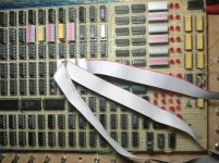
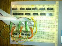
001.jpg 003.jpg

THANK YOU Marty
 
Last edited:
Marty,

Rotating the accumulator has nothing to do at all with the ALU - it is all handled using the serial shift function of the 74194. Again, have a look at my 74194 schematic and check it out with your wiring.

CIN also has no bearing on rotating - it is the LINK register that is rotated in. The ALU is only loaded into the accumulator when the AC(L) signal is active (low). Setting this permanently HIGH will inhibit parallel loading (so that will avoid any confusion).

There are two signals (S1 and S0) that control the accumulator. 00 = Do nothing, 01 = rotate right, 10 = rotate left and 11 = load from ALU. RAL, RAR and AC(L) are decoded by a couple of gates to produce the S1 and S0 signals for the 74194s

One thing to remember - the Accumulator contains a clock signal and as long as RAR or RAL is there the ACC will be rotating once every clock cycle. Therefore RAR and RAL need to be active for one clock cycle - otherwise multiple rotates will occur. Also beware that you need fully debounced signals. What is not shown on the LD12 schematics is that all of the switches were debounced on the panel interface. If a signal 'bounces' - you will get unpredictable behaviour. All of the edges must be 'clean'.

Dave
 
Last edited:
Hi All;

Dave Thanks for Your reply.. And informative answers..

"" Rotating the accumulator has nothing to do at all with the ALU - it is all handled using the serial shift function of the 74194. Again, have a look at my 74194 schematic and check it out with your wiring. ""
I knew this.. I just have to find Your 74194 Schematic..

"" CIN also has no bearing on rotating - it is the LINK register that is rotated in. The ALU is only loaded into the accumulator when the AC(L) signal is active (low). Setting this permanently HIGH will inhibit parallel loading (so that will avoid any confusion). ""
"" CIN also has no bearing on rotating ""
I know that, But Cin does have bearing of the Alu doing an increment, and my thought was that if it was doing a Rotate and an increment at the same time.. I have not proved that at present, just a guess in the early morning..

"" There are two signals (S1 and S0) that control the accumulator. 00 = Do nothing, 01 = rotate right, 10 = rotate left and 11 = load from ALU. RAL, RAR and AC(L) are decoded by a couple of gates to produce the S1 and S0 signals for the 74194s ""
I knew about both things..

"" One thing to remember - the Accumulator contains a clock signal and as long as RAR or RAL is there the ACC will be rotating once every clock cycle. Therefore RAR and RAL need to be active for one clock cycle - otherwise multiple rotates will occur. Also beware that you need fully debounced signals. What is not shown on the LD12 schematics is that all of the switches were debounced on the panel interface. If a signal 'bounces' - you will get unpredictable behaviour. All of the edges must be 'clean'. ""
This might be the main or possibly another reason for my troubles.. I was hoping, since that was how I had it when I first implemented the first board, that I could get away with not having debounced switches, I did have it on some switches, later on..
I would need to find another Board to put them on for this machine, as I have NO room in the inn for more Ic's..
Tomorrow will tell..

Dave, on another side note, Could You send me, you file/schematic for Your Microcoded PDP 8 machine, I am curious what all it has in it.. Thank You..

THANK YOU Marty
 
Last edited:
Hi All;

I Found out what I was doing Wrong, with the 74194's, I had un-wired all of the pins 2 and 7.. And That is what was causing the confusion in the 74194, Pin 2 or pin 7 depending on the direction of the shift, would shift in a (1) high, and thereby causing the bits to eventually fill up..
I had added some Led's to my BreadBoard, which I used first on the inputs, which proved, that they were not the problem, So I changed them to the outputs, and dis-attached the outputs from the extender cable, and they did the same thing..
I then had an inspiration, and connected pin 2 to pin 15, and pin 7 to pin 12, that didn't work, so I exchanged them, pin 2 to pin 12 and pin 7 to pin 15 and it worked..
Now to do the same thing with all three 74194's, and work out who connects to whom.. Before putting in the Link Bit..
Which brings up another thing, I am going to need to look at the 74109, J,K flip-flop in the Lab Manual, and figure out "how" to set and reset it, I had problems with this in the Old machine.. I made a different circuit that would work, and later changed it back to the original.. But, it is one Flip-flop I have had problems with, and need to figure out "how" to make it work, and work reliably..

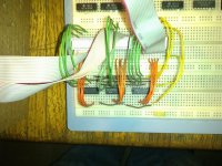
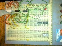
001.jpg

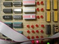
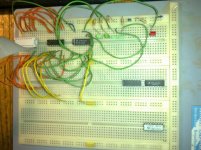
I have wired up the 74194's on the BreadBoard, and successfully made the Bit Shift both Right and Left.. In the picture it shows a single Bit since it is not a moving picture, along with the associated circuitry..

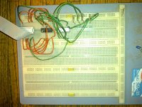
003.jpg 002.jpg

Next is wiring up the 74194's on the System, and making sure it works there as well, before Tackling the problem of the 74109..
Next is wiring up the 74194's on the System, That now works, all wired up..

THANK YOU Marty
 
Last edited:
My PDP-8i Microcode implementation

My PDP-8i Microcode implementation

Marty,

My bad - I thought I had updated them a while ago. Clearly I hadn't...

8imc_copy contains the microcode (the build and run files for my iMac plus the JAVA source code and resulting class file to build the microcode required for my LOGISIM MICROCODE ROM (also included pre-built)). If you want to understand the microcode - just have a look at PDP8i_MICROCODE.java. The microcode itself 'starts' just after the method main. It'll probably seem like gibberish - but I can explain it to you if you need an explanation.

The LOGISIM file is located within 8ilogisim_copy. You should notice that the 'hardware' requirement for the microcoded solution is much simpler than the LD12 - as a lot of the 'logic complexity' has been incorporated into the microcode decision logic itself. The microcode 'architecture' is pretty much the same as the LD12 - with the registers, ALU, MUX and a bit of support logic to ease the decision making within the microcode (i.e. the microcode may decide to jump upon whether a status flag is true or false. The status flag itself is derived from a bit of hard-wired logic - however this logic is kept to the bare minimum).

Dave
 

Attachments

  • 8imc_copy.zip
    17.2 KB · Views: 3
  • 8ilogisim_copy.zip
    80.7 KB · Views: 3
Last edited:
Great to see that you are now shifting...

The 74109 is quite simple if you look at the truth table on page 1 at http://www.ti.com/lit/ds/symlink/sn74109.pdf.

There is a /PREset and a /CLEar input. These signals should both be normally high. Pull /PREset low to set the Q output to a '1' (the /Q output will go to a '0'). Pull /CLEar low to clear the Q output to a '0' (the /Q output will go to a '1'). Do NOT set both the /PREset and /CLEar low simultaneously!

When /PREset and /CLEar are both high - the Q and /Q follow a simple truth table on the low to high transition of the input CLocK:

J /K
0 0 - Output Q will be set low ('0').
0 1 - Output Q will not change it's state.
1 0 - Output Q will toggle its state (from a '0' to a '1' or the other way).
1 1 - Output Q will be set high ('1').

In all cases the /Q output will be the inverse state of the Q output.

Keep up the good work - you will get there!

Dave
 
Hi All;

Thank You Dave for the great files, I will look at them in a minute, and the Explanation of the 74109..
I looked it up in the Lab Manual, for the information..

"" Great to see that you are now shifting... ""
I know I am a shifty kind of guy..

I have hooked up on the Lower pins 1 through 7, only pin 4 for Clock, and Power and Ground, and I can take pins 1, 2, 3 and 5 to Ground when needed..
I have some Led's tied to pins 2 and 3 and 6 and 7 to show input and output..
So, far in three Ic's, I can get pin 6 to go High or Low, BUT, pin 7 is ALWAYS High.. And the only thing wired to it is an LED Driver, I could change that out and make sure that is not the problem..

004.jpg 005.jpg

I have some New 74109's coming sometime this afternoon, that I can also try..

THANK YOU Marty
 
Last edited:
Hmmmm.

Pin 7 should always be the opposite state of pin 6 (except when both pins 1 and 5 are low simultaneously - in which case the output of both pins 6 and 7 is somewhat indeterminate).

Just to state the obvious - you do have 10 kOhm (or similar) pull-up resistors on input pins 1 through 5 don't you? i.e. don't let any of the input pins float.

Dave
 
Hi All;

Dave, Thank You for Your answer..

"" Just to state the obvious - you do have 10 kOhm (or similar) pull-up resistors on input pins 1 through 5 don't you? i.e. don't let any of the input pins float. ""

NO, I didn't know it was needed..

Do, I need this only for this setup or/and do I need this for the rest of the 74109's in the circuits, on the main system ???

I don't have any 10K ohm resistors in the system anywhere..

Putting in the 10K Rpack, (I need to make sure it is a good one) made no difference.. Yes, they all measure 9.87K or so..
THANK YOU Marty
 
Last edited:
I was just talking about when the 74109 was on the breadboard - not in the '8'.

You said "... I can take pins 1, 2, 3 and 5 to Ground when needed". If you don't ground the pins - what is the state? If the pin is not connected to anything it will float (i.e. the logic value of the input is indeterminate). You should have all input pins connected to a 10 kOhm pull-up resistor (one per input pin) and then ground the pins as desired. Unconnected input pins are therefore pulled high if not grounded. I see you have a ribbon cable connected to the upper-left of your breadboard and I can't see how the inputs are wired - so you may have other things connected to the inputs via the ribbon cable?

Dave
 
Hi All;

Dave, Thank You for Your answer..

"" I was just talking about when the 74109 was on the breadboard - not in the '8'. ""

OK !!!!!

"" You said "... I can take pins 1, 2, 3 and 5 to Ground when needed". If you don't ground the pins - what is the state? ""
I have put a 10K ohm rpack connected to pins 1, 2, 3, and 5.. As I stated in posting #110..

"" I see you have a ribbon cable connected to the upper-left of your breadboard and I can't see how the inputs are wired - so you may have other things connected to the inputs via the ribbon cable? ""

At Present the cable is for Power, Ground and Clock, Nothing else is connected to it..
I had hoped to eventually have it so I can connect it to the "System", I did have it connected with all of the inputs and outputs from the System, using the Led's for a status on pins 2 and 3, and outputs 6 and 7.. And after seeing a problem, I reduced it to Power and Ground and the Clock..

I just got the IC's from the supplier, and I tried one of the new ones..
Same Result..

THANK YOU Marty
 
Last edited:
Odd...

Try a 74109 on its own.

Pin 8 = 0V (GND)
Pin 16 = +5V (VCC)
Pin 1 = 0V (/CLR)
Pin 5 = +5V (/PRE)
Leave pins 2, 3 and 4 open circuit (the state doesn't matter whilst the chip is being cleared or preset).

Output pin 6 (Q) should be at 0V (Pin 1 is clearing the Q output).
Output pin 7 (/Q) should be at +5V (ish).

If not - something is really wrong with reality!

Dave
 
Hi All;

Dave, Thanks for the Help..

""
Try a 74109 on its own.

Pin 8 = 0V (GND)
Pin 16 = +5V (VCC)
Pin 1 = 0V (/CLR)
Pin 5 = +5V (/PRE)
Leave pins 2, 3 and 4 open circuit (the state doesn't matter whilst the chip is being cleared or preset).

Output pin 6 (Q) should be at 0V (Pin 1 is clearing the Q output).
Output pin 7 (/Q) should be at +5V (ish). ""

I did this and I got the Same as always (before), OK, so this works..

I then tied pin 1 to +5 and Pin 5 to Ground..
SUCCESS !!!! Pin 7 goes LOW...

Now, If I connect it with a clock and pins 2 and 3 first tied Low and then tied High, it should be able to do the same thing..
I just noticed something, when I went back and looked at Your table..
"" When /PREset and /CLEar are both high - the Q and /Q follow a simple truth table on the low to high transition of the input CLocK:

J /K
0 0 - Output Q will be set low ('0').
0 1 - Output Q will not change it's state.
1 0 - Output Q will toggle its state (from a '0' to a '1' or the other way).
1 1 - Output Q will be set high ('1').

In all cases the /Q output will be the inverse state of the Q output. ""

"" When /PREset and /CLEar are both high. ""
I can't say I had Both tied High.. I will retry..

THANK YOU Marty
 
/PREset or /CLEar going low will override anything else you do with the J, /K and CLK inputs.

If /PREset and /CLEar are both low - then both the Q and /Q outputs are 'sort of high' simultaneously.

Dave
 
Hi All;

Dave, Thanks for Your Help and suggestions..
I just tried it, with both Preset and Clear, both set to high..
And just in case, I used my Digital Pulser for a clock.. (Radio Shack)
I even pulled pin 4 up with a 10K resistor (Rpack)..
So, there is a pull-up on pins 1, 2, 3, 4 and 5..
I tried all combinations for pins 2 and 3..
And Nothing works, as far as making pin 7 go low, pin 6 goes Low and pin 7 stays high.. Same as before..

I Just got it to Work !!!!!!!!!!!!!!


I found when pulling the wires from the cable, I had thought I had, all the cables pulled, but I didn't.. Pin 1 in the cable was still connected to pin 1 on the IC..

This brings me to another Issue that I need to look into..
Pin 1 is connected to CLL, and it should be High, but it is not.. So, I need to look into that, before I can made the Link Bit Work..
I think I have found the problem, with CLL, the Clpr.L is tied to Clpr.H instead..

It Now shifts thru and includes the Link Bit, using the 74109.. So, this is fixed..

THANK YOU Dave for Patiently working me through this..

Dave, on another side Issue, I Plan on after I get this (hopefully) working to wire-wrap Your Micro-code PDP 8i clone.. On a different Board..
What can I say I am a glutton for punishment..

THANK YOU Marty
 
Last edited:
Hi All;

Dave, I have a strange, but, Maybe problem -- solution to my System..

I have been trying to get some of the 7xxx commands to work.. Like RAR, RAL, etc..
I had been looking at numerous one's comparing them.. Like with RAR and RAL, I could get them to work, If I used my Pulser or clipped a signal High or Low depending on where it was.. And then the command would work..
And look at the CML command and finding the same kind of results.. I could make it work, If I changed an output..
So, I somehow decided to change OPG1.H, to OPG1.L, with a jumper wire and a bent pin..
And the circuit worked !!!!
I then did the Same thing with RAR and it worked as well..
SO, I used my BreadBoard, and I took the signal out of the 7402 (equivalent to M2, pin 1) and put it through an inverter (7404)..
And as much as I have checked, the commands like RAR, CLL, CML, etc. all work !!!!!!
Now I can't say about any regular commands like AND, TAD , as I haven't tried them..

This according to both the original Schematic, Your Schematic, it should NOT work, but, it does work ?????

THANK YOU Marty
 
Hi All;

I have put in a small program, And I attempted to Run it..
0000 7320 CLA, CLL, CML
0001 7001 INR
0002 7010 RAR
0003 5000 JMP to 0000
It works for a time or two, but it then goes past the program and executes whatever is there in memory..
I changed the above program and it works better.. The Link Bit does turn on and off.. And it is Jumping back to '0000..
0000 7320 CLA, CLL, CML
0001 7001 INR
0002 7020 CML
0003 5000 JMP to 0000
It still goes into the weeds, after a few runs..
The program is still in Memory, it is just going past it's boundaries..
So, a jump instruction may or may not completely work..
I don't know, but maybe, PC(L) needs to be Looked at more carefully..
I haven't yet, tried the program in single step mode, to see what is happening..

THANK YOU Marty
 
Last edited:
Excellent news about the 74109.

I thought there were too many wires on that breadboard for my liking...

And yes I do think you are a glutton for punishment in having a go at my microcoded solution - but I admire your determination!

Do ***NOT*** just randomly change wiring around for no apparent reason. You will ultimately regret it as you ***WILL*** have to undo the work you do in the long run!

Let us assume for the time being that the 7442 decoder (L5) - or some of the surrounding logic - is not working properly and (as a result) all of the /0 to /7 outputs are 'high' irrespective of what instruction is placed into IR<0..2>.

During the EXECUTE phase - none of the instructions will be decoded by the 7442 (due to our postulated fault) and none of the logic will work correctly as a result. Even if IR<0..2> contains binary '111' - indicating a 7xxx instruction - L5 pin 9 (/7) will never go low. In this situation, if you swap OPG1.H for OPG1.L you are mistakingly thinking that this is fixing your problem as the OPG1 instruction now seems to work. However, if you put binary '000' (an AND instruction) into IR<0..2>; the OPG1 instruction will still be executed! This is clearly incorrect!

When (ultimately) you identify and fix the root cause of the problem with L5 - this will now cause your OPG1 instruction to stop working as you have inverted OPG1.H and OPG1.L. L5 will decode the instruction correctly and the extra inverter that you have added will cause the signal to become the wrong way round. In fact it is worse than that - because every instruction other than a 7xxx will also cause the 7xxx instruction to be executed at the same time! Clearly this is worse...

By all means 'play' with signals to see what the effect is - but because something starts to work I wouldn't make the change 'permanent' until you identify the theory behind why it is working now and wasn't before.

I think you have already identified what I have said with your statement "This according to both the original Schematic, Your Schematic, it should NOT work, but, it does work ?????".

It only works by accident - not by design!

If you have 20 faults in your wiring you can end up going down quite a few "dead ends". As I have said before (sorry to keep labouring the point) your debugging needs to be 100% methodical so that you fix 1 bug, then the next, then the next and so on. It's a painful process - but the only one. If you introduce what you think (in error) is a bug fix - you have just created yourself a new bug for the future instead of fixing one now.

Dave
 
If you put '111' in IR<0..2> (a 7xxx instruction) do you see L5 pin 9 (/7 output) go low during the EXECUTE phase of your instruction? If not, do any of the other outputs from L5 go low (especially pin 5 - /JMS)? I have a reason for asking this - as I got the sense of my MUX gate input wrong (L6 pin 1) when I did my LOGISIM implementation.

L5 pin 12 (D input) should be low and L5 pins 15, 14 and 13 should follow IR<0..2>. When you are loading values into the IR - do you correctly see IR<0..2> appearing at L5 inputs A, B and C. If not - you need to find out why not.

Dave
 
Back
Top