• Please review our updated Terms and Rules here
  • From now on we will require that a prefix is set for any items in the sales area. We have created regions and locations for this. We also require that you select a delivery option before posting your listing. This will hopefully help us streamline the things that get listed for sales here and help local people better advertise their items, especially for local only sales. New sales rules are also coming, so stay tuned.

Z80 SIO/1 and 628128 RAM wanted for Z80 CP/M project

Stephen Scutt

Member
Joined
Sep 9, 2015
Messages
22
Hi everyone. I recently bought a PCB on Ebay which is a Z80 SBC based upon Grant Searle's Z80 CP/M breadboard project: http://searle.hostei.com/grant/cpm/index.html
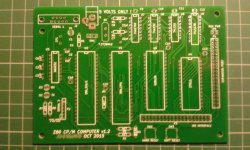

z80board.jpg

I would like to know if anyone in the UK (or anywhere really) has a Z80 SIO/1 chip and a 62128 SRAM chip (32 pin DIP) they could sell me for a reasonable price or donate towards the project..

If you do please send a message.

Any help seriously appreciated.

Thanks,

Steve.S
 
Few Z80 applications actually used the synchronous facility of the SIO, so Zilog disabled that part of the SIO and marketed it as the Z80 DART. Pin compatible; software can't tell the difference--and quite plentiful. I've got a drawer full of the little buggers.
 
Few Z80 applications actually used the synchronous facility of the SIO, so Zilog disabled that part of the SIO and marketed it as the Z80 DART. Pin compatible; software can't tell the difference--and quite plentiful. I've got a drawer full of the little buggers.

From distant memory there were several pinouts of the SIO, and I believe the Dart was the equivalent of the SIO/0. It's worth a quick look at the schematic to compare.

In any case, here in the USA www.unicornelectronics.com has both the Z80-SIO/1 and 128Kx8 SRAM very inexpensively - it's the shipping that will be costly.
 
Yes, Zilog chip designers didn't have enough pins in a 40-pin DIP to get all the handshaking signals out. The problem was that there were 4 signals and 3 pins. Since the engineers couldn't make up their hive mind, they offered the chip in three different bond-outs.

So there was the SIO/0 SIO/1 and SIO/2, which were all bonding options. The /0 joins the pins for receive and transmit clocks for the B channel together; the /1 separates them, but loses the transmit buffer status on the B channel. The /2 separates the clocks and keeps the transmit buffer status, but loses the SYNCB (sync byte detected) output.

Since you're likely to be sending at the same rate you're receiving, the /0 and DART make the most sense. In any case, converting between them is very minor and doesn't involve tinkering with the software in most cases. Many Amstrad CPC boxes used the DART.
 
Hi Steve

Please tell me more about this pcb from Grant Searle. I know the schematic, but I am
very imtersted to buy this pcb. Have you more infos about the seller?

Regards
Thomas
 
Back
Top