• Please review our updated Terms and Rules here

The Datapoint 5500 thread..

jdreesen

Experienced Member
Joined
Jul 5, 2012
Messages
414
Location
Switzerland
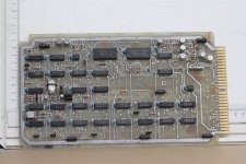
As I have been loaned (thanks Jaak Bartok !) a Datapoint 5500, with the target of gettting it running again, I thought this might be a good spot to track progress.

The 5500 is a follow-up of the 2200, and shares the same housing. Internally it differs quite a lot from the 2200 : while ALU is almost identical, and PC/stack is very similar, though with added MMU, the control logic is very different.
The DP5500 is a microcoded machine,, with 10 256x4 proms defining the functionality. (The 2200 has hardcoded logic.)
Additionally the 5500 contains 4K of firmware code.
The 5500 shares the PSU and the display-card with late models DP2200.

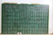
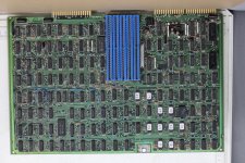
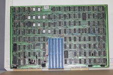
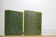
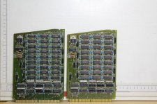
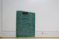
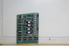
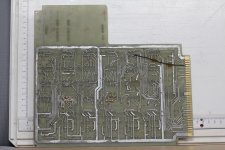
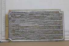
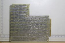
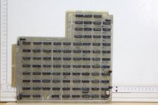
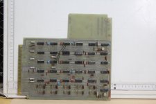
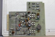
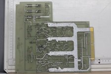
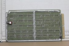
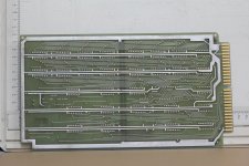
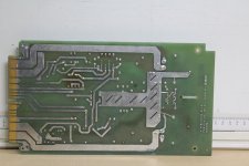
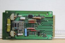
PCB pics will follow, but let me start off with some reengineered schematics and rom-recoveries.
(The .tar.txt is actrually a tar file)

Thanks to Ruud Balstissen for extensive pre-work on the schematic.

Jos
 

Attachments

  • DP5500_ram_rom.pdf
    276 KB · Views: 9
  • DP5500_mb.pdf
    1.9 MB · Views: 11
  • DP5500_PSU.pdf
    168 KB · Views: 1
  • dp5500roms.tar.txt
    30 KB · Views: 5
FYI, I was looking at the firmware roms, all the bits are inverted (negative logic), just in case that saves someone some time.
 
Bruce is indeed correct : the 4 firmware proms ( and only those) are negative logic.
The ROMS as posted above are the actual contents of the ROMs themselves.
In general the internal databus is present in negative and positive logic. The external IO bus is negative logic.
The memory cards are inverting, if you look at the memory card you will see an inverting buffer after the firmware ROMS.

If you are debugging a DP5500 it might be useful to look at the main buffer between negative and positive logic : IC97 This has testpin E1 associated with it. Grounding E1 will isolate the databus and allow you to feed in external signals. This was used to read out ROMS 61 & 62
 
Thanks for the schematics, Jos!

There are a number of things that you can perhaps change to make it clearer:
  • Z25A output is Q and ~Q. It would be great if the signal was ra8 and ~ra8, not ra9. It give an impression that the microaddress bus is 10 bits but it is in fact 9 bits.
  • I cannot seem to find the ns9 signal. The bus is marked ns[9..0] but as far as I can see there is no ns9 anywhere? ns8 seems to be the highest which makes sense since the microaddress bus is 9 bits then next state bus should be 9 bits.
A very odd design IMHO. The sequencer seems to use a 9 bit microaddress for 512 microinstructions. There is no pipeline register for the ctl-outputs which I would have expected. The ns bus seems to be used for microjumps. Z61 and Z62 seems to take the input directly from the databus. Some kind of lookup for something?
 
I will update the schematic as you suggest, but I will wait until I have the rest of the machine covered ( backplane and decoder III board )
Keep in mind that these schematics are created from the sounding out the PCB. There are bound to be some errors....But all TTL IC's are covered.

Z61 and Z62 are read out whenever interrupts are pending. I do not really understand how it works, also start/stop/single stepping is unclear to me.
 
That intr signal seems to be active high. The 74148 ~EO signal is high if any of the input I0 to I7 is low. The enable inputs for the PROMs are active low so if I am not mistaken Z61 and Z62 is active when there is no interrupt, or?
 
Another odd thing is the ns1-ns3 signals which are both driven by three OC NAND gates (Z31) and also Z23 and Z23 82S129 three-state bipolar PROMs. OC-drivers and TS on the same bus? It is a good thing to make sure that they aren't driving against each other. Thus the intr signal has to low (inactive) while cmdb7 and ck_aa is high (active), but intr looks quite independent. One has to simulate all those clocksignals to figure exactly when intr is active.

If the PROMs were a 82S126 pushing them on the same bus like this could have enabled microjumps on different interrupt-levels. The PROMs are really the TS 82S129 and not the OC 82S126, right?

Looking a bit more at the microcode state machine it looks like Z61 and Z62 is an entrypoint generator that is mapping instructions into entrypoints in the microprogram which it jumps to when doing a fetch. The actual micro program is 16 bits wide with a jump address part (ns) and control signal part (ctl). The ns0 to ns3 is also decoded into control flags when not used for jumping. Haven't figured out when the ns part gets loaded into the micro-PC, though.
 
The ROM's are MMI6301-1, and yes, tristate and OC are indeed mixed...
There is the additional "decoder iii" board that also contains some of the clocking circuitry, still need to draw out that.

I can send you the Kicad project if that eases things.

Z61 and Z62 as an entrypoint generator is probably right, the only register clear identifiable as an instructionregister is only 6 bit wide (Z80, a 74174)...
 
Aha. Then the 3bit wire-or of the ns1..ns3 makes perfectly sense since it would provide some kind of micro-jump based on interruptlevel.

Perhaps you can put the schematic in a github repo so that more people can contribute?

Actually a 6 bit IR makes sense since the upper two bits identify the instruction group in the 2200 instruction set. The six lower bits may indicate a source and/or destination register.
 
Has anyone figured out at what address in the 4k firmware it starts at power up? There seems to be 10 jumps in the first 30 locations in the firmware file. It could be the nine interrupt vectors and then one additional?

I checked the 5500 but I couldn't find the info in there.
 
Got sidetracked by other projects....
Aren't these jumnps described in the 5500 hardware manual, page 10 ?
 
I checked page 10 but cannot find the entrypoint for powerup and restart. Maybe I am looking in the wrong page? I tested a bunch of entries and the last one I tested got me to a routine that is setting up the sector table.

Now I have to add all that memory managment stuff which got me into refactoring the entire memory-subsystem.
 
Some pics of the mainboard....
 

Attachments

  • main_b.jpg
    main_b.jpg
    1.6 MB · Views: 5
  • main_f_2.jpg
    main_f_2.jpg
    1.7 MB · Views: 5
  • main_f.jpg
    main_f.jpg
    3.9 MB · Views: 5
....memory boards...
 

Attachments

  • ram_b.jpg
    ram_b.jpg
    6.6 MB · Views: 4
  • ram_f.jpg
    ram_f.jpg
    6.7 MB · Views: 5
  • ramrom_b.jpg
    ramrom_b.jpg
    6.2 MB · Views: 4
  • ramrom_f.jpg
    ramrom_f.jpg
    6.1 MB · Views: 4
Decoder, Keyboard driver, display board....
 

Attachments

  • keybrd_b.jpg
    keybrd_b.jpg
    7.3 MB · Views: 3
  • decoder_f.jpg
    decoder_f.jpg
    6.2 MB · Views: 2
  • decoder_b.jpg
    decoder_b.jpg
    7.3 MB · Views: 2
  • disb_b.jpg
    disb_b.jpg
    7.2 MB · Views: 2
  • disp_f.jpg
    disp_f.jpg
    6.6 MB · Views: 2
  • keybrd_f.jpg
    keybrd_f.jpg
    5.7 MB · Views: 2
...and the rest... ( yes the bootboard only has a switch on it...)
 

Attachments

  • defl_amp_f.jpg
    defl_amp_f.jpg
    6.2 MB · Views: 4
  • defl_amp_b.jpg
    defl_amp_b.jpg
    6.9 MB · Views: 4
  • boot_f.jpg
    boot_f.jpg
    7.3 MB · Views: 4
  • boot_b.jpg
    boot_b.jpg
    7.3 MB · Views: 4
  • pwr_b.jpg
    pwr_b.jpg
    5.9 MB · Views: 4
  • pwr_f.jpg
    pwr_f.jpg
    6.4 MB · Views: 4
I have been adding 5500 features to my simulator. It now has the 4k ROM present that Jos dumped in 17xxxx area if you enable 5500 CPU (set cpu=5500). After some research of this ROM I found the ROM vectors for interrupts that the machine traps to along with the powerup-vector:

// 170000 (167400) Memory parity Failure Vector
// 170003 (167406) Input Parity Failure Vector
// 170006 (167414) Output Parity Failure Vector
// 170011 (167422) Write Protect Violation Vector
// 170014 (167430) Access Protect Violation Vector
// 170017 (167436) Priviledged Instruction Violation Vector
// 170022 (167444) One Millisecond Clock Vector
// 170025 (167452) User System Call Vector
// 170030 (167460) Breakpoint Vector
// 170033 Jumps to HALT!
// 170036 Startup routine most likely

The startup routine initializes the sector table and base register so I implemented those as well as well as memory protection (ROM is always read-only, of course)
This routine then goes on to what looks like a memory test and then finally loads the character generator (which is not simulated except for allowing it to happen). Then it halts. According to the manual that look like the intended behaviour.

However somewhere there has to be a Boot-routine which is supposed to be executed automatically when the machine halts (after it has powered-up). I cannot find the entry point for that one. I have stepped through some subroutines and ended up in one that seemed to take input from the keyboard.

Jos, do you have any ideas on where the Boot-routine is located? Could it be found from the micro-code / schematic somehow? It is tedious to map out the ROM by stepping through / running subroutines..

Screenshot 2024-02-19 at 19.27.37.png

The disassembler is now driven by a tab-separated document that is converted into a c-header for inclusion in the project. All (most at least) 5500 instructions should now be able to be disassembled correctly and all except a couple of instruction in the 5500 is implemented. I get to those when I see them.
 
Not sure what you mean by boot-routine. The initial loading from a mass storage device ? The manual describes this as the "restart" operation ( appendix A)
There we will need to check the firmware to locate that call. The machine I took the ROM from does not have tapes, therefore there must be some call to one of the disk-drive options.

But I don't know a startaddress, sorry...
Could it be just after the "halt" of 170033? because if the "auto restart" switch inside the machine is on ( it normally is) then the machine will not halt but just continue running. At least that is how I understand it.
 
The power up routine starts at 170036. I tried to analyze the first 2k but haven’t yet found any boot-routines/restart-routines Need to check the rest to see if I find the restart routine.

But somewhere the constants for the various entrypoints that the machine moves into the program counter has to be stored. I wonder if it is in the microprogram or somewhere else. It can perhaps be a way of finding them rather than searching trough the code?

Based on the fact that this machine doesn’t have tape tou mean that it boots ditectly of disk. Floppy disk or 9370 disk or other?
Then perhaps there were different firmware for different versions of the 5500? Those with tapes and those without tapes.
 
I used my simulator to get a trace of the execution and then filtered using some unix tools like sort, uniq and cut. I iterated this process a number of times trying to track down all missing paths in the code and finally got a decent listing out of it. It is possible to identify sections that are related to tape and diagnostics. It is evident the ROM is not only meant for the 5500 but later models which could have more memory as well since text says 124K etc and there are 6600 unique instructions in the code (which are NOP in the 5500).

The file is here: https://github.com/MattisLind/DP2200/blob/main/dp2200sim/datapoint_5500_ROM_disassembly.lst

Please contribute and try to de-cipher the code!
 
Last edited:
Back
Top