Edited this post for errors.
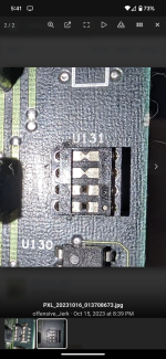
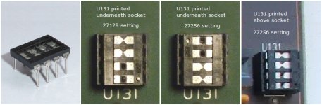
It seems even though my board has U131 printed above the socket, it still uses the configuration for the boards with the printing below the socket.
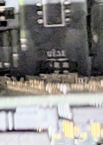
I found a picture of my board before I wrecked the U131 socket. It is a terrible picture, but I was not trying to take a picture of U131. By default, the top pins were not bridged, so when I put a solder bridge on the bottom pins, I didn't actually change out of 27256 mode, as it was the same configuration as default.
This must be why I could not boot with only two of the award/phoenix roms (but it did boot with three).
The third picture of U131 with the repaired socket and top two pairs of pins bridged was the mode where I actually was getting the correct address locations and where I did not get a parity error when dumping the ROMs. This was after I repaired the socket.
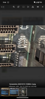
The last picture is after I destroyed the socket and solder bridged the bottom pair on pins, and was getting the bios address mismatches, with was the same as the default 27256 mode.
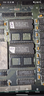
The picture of the IBM ROMs was a reference photo I took before I made any changes.