• Please review our updated Terms and Rules here

6560 (and 6502) manufacturing technology

Kakemoms

Experienced Member
Joined
Aug 25, 2016
Messages
125
Location
Norway, Europe
Hi

I am trying to find out more about how the different revisions of the original MOS6560 (VIC) chip was manufactured. It was designed in 1975-1977, so I guess it started out with hand layout on paper and Rubylith, but by the last batch (1984) it must have gone through some transitions. Was it digitized? Translated into VHDL? If anyone here knows anything about how MOS design and photomask manufacturing changed in the 1977-1983 period, I would like to hear about it.
 
Many more videos here - Not just about MOS Technology the company but the technology too. So a bit of filtering the content you'd be interested in.

http://www.mashpedia.com/MOS_Technology

Thanks. I had already found the Commodore factory tour video on youtube and were able to deduce some information from that. On 6502.org I posted this:
I was actually able to find out several things from this old factory tour video:
https://m.youtube.com/watch?v=xu8Fi0tC9IA

Its from around 1982-1983 and we can see some really large terminals, grapical layout and big paper plots. No vhdl there. Its also possible to see that the engineer works on a "7520" which never reached the market.. The cleanroom shots with yellow light shows several steppers and we are also shown a reticle (used in projection aligners).

A nice factory, quite up to date, but unfortunately everything made on 4inc which in the long run was an expensive process (especially for the larger Amiga chips). Equipment cost for going to smaller transistors were also increasing exponentially, which would have needed a considerable investment by around 1986-1987. I don't know if that factory ever got to 6 inc, or was just closed down by that time.

I see that the page you linked to says "GMT (Microelectronics) would have provided foundry services based on TelCom's Bipolar and SiCr Thin Film Resistor processes and would have been licensed alternate sources for TelCom's Bipolar based products., with production running at 10 thousand 5-inch wafers per month, producing CMOS, BiCMOS, NMOS, bipolar and SOI devices."
It doesn´t reference any sources for this information, and I would be surprised if they went to 5inc instead of 6inc at that time.

I got a response from BigEd on 6502.org as well:
That fits my experience. In the mid-80s we were using Calma 2 workstations, where you could directly enter and edit layout, and there was at least one remaining Calma 1 unit, which I think was more about digitising from drawings - there was still a rank of giant drafting boards.

We did describe our designs in a simulation language so we could do logic simulation, but there was no direct link to layout - no synthesis. When I first used synthesis technology, probably in the early 90s, the software was already very expensive, and it only got more expensive as time went on. (There was some logic minimisation software from the academic world which was free, and that helped if you had a PLA or similar regular logic implementation.)

I found some interesting information from a 1987 industry report on semiconductor manufacturing that shows many things. Originally the MOS factory line must have been around 3-10um, probably with Perkin Elmer aligners, with improvements happening on a steady basis. From my involvement with the decap and imaging of the early 6560, we see that this seems to be about right.

At the introduction of Amiga (OCS) chipset, the gate width was probably around 2um (this is the HMOS-II spec), which corresponds nicely with the 6MHz speed.

I´m surprised there are no MOS technology people around on these sites. I know it was 30 years ago, but some of them should still be around..?
 
Last edited:
The 6502 started on an 8um process, according to Wikipedia.

https://en.m.wikipedia.org/wiki/List_of_semiconductor_scale_examples

Quotes from engineers in Brian Bagnals books note a shrink to 5um, and the original Amiga chipset was done at 3um. After the 3um process they installed a CMOS production line as well for the Fat Agnus (NMOS/HMOS) was used prior.

By the time they got the AGA chips they contracted out, so I don’t know if MOS got below 3um.

It is frustrating the lack of detail on this stuff.
 
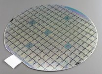
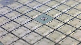
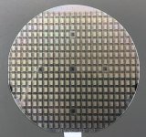
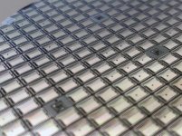
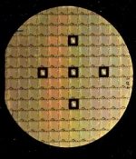
Well, just to follow this up a little bit. I recently bought a 6569R5 wafer from someone on ebay. It is a full 4 inc/100 mm (pick your choice) wafer with 6569R5 chips. I am not sure if some of them are marked (bad ones), so this may have came out from before device testing. There is also 5 smaller chips on it, which are probably a test run of some other component. It looks like it has been decently stored.

The 4 inc wafer is the reason Commodore made very little money. Compared to 6 inc process, 4 inc was much more expensive per chip to run. A contemporary report from Intel shows this really well. Looking at the wafer we can see that its only about 250 chips on them as the 6569 is quite large.

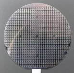
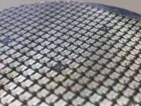
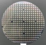
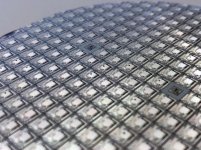
I also include some other wafer pictures from MOS. All made in 1984 or later on 4 inc. In fact, one (dma controller) seems to be an Amiga component used in the A2090 scsi controller which was sold from 1988.

All-in-all this seems to indicate that Commodore stuck to their 4 inc process into the late 1988. Not surprising since they had little money at the time, and it looks like they neither put capital aside to replace the fading 4 inc process.

6569R5-1986-wafer.jpg
6569R5-1986-wafer1.jpg
MOS 6569R5 VIC-II wafer

6526R3-triport-1984-wafer.jpg
6526R3-triport-1984-wafer1.jpg
MOS 6526R3 CIA wafer

8721R3-1984-pla-wafer.jpg
8721R3-1984-pla-wafer1.jpg
MOS 8721R3 PLA wafer

8727R3-dma-1984-wafer.jpg
8727R3-dma-1984-wafer1.jpg
MOS 8727R3 DMA wafer
 
Last edited:
Any chance you could cut a TRIPORT out for me and bond it to a package? :)

Actually I thought the 6526 was the CIA.

One a more serious note, I believe I have read before that MOS/CSG never progressed beyond 4" wafers, so your deduction is likely correct!
 
You are correct.. its the CIA interface chip used in C64.

Heh.. even if it was the Triport chip, I doubt I could have done that.. getting hold of packages for example is not so easy. Finding which pad to bond to which wire even less so..
The rest of the equipment I do have access to ;)

Edit: After contacting the seller, he has confirmed that this is in fact the 6525 Triport interface and not the 6526. (but for some reason I can't edit the above post). I have bought that wafer as well, so once it arrives in a couple of weeks I will look at it myself (under a microscope). In interesting, but a little sad fact is that a large number of devices on the 6525 wafer seems to be marked as non-working (see ink marks).
 
Last edited:
Just to follow up a bit, a MOS2050 SRAM wafer ( apparently from 1970) can be seen as a 2inch wafer here:
5585FE6E-44BA-4915-B11C-4261E1DAE3A2.jpg

I haven’t found a datasheet for this component, but a later 1Kbit (256x4) appear in the 1976 catalog.
 
Back
Top