• Please review our updated Terms and Rules here

Compact Flash with true 8-bit XT IDE Interface

As I identified in my first post on this thread, there are four Tandy 1000 machines which use an 8-bit IDE port, the TL/2, TL/3, RL and RLX. The port only puts out A0 and A1, but true AT IDE requires A2, so that line will need to be connected from an ISA slot. I believe the latest builds of the Universal XT-IDE BIOS supports 8-bit CF transfer modes, so no latching hardware will be required.

To avoid having to use an expansion card for the Universal XT-IDE BIOS, the code will have to be added to the existing BIOS ROM. Earlier Tandys, the TL, SL and SL/2 used two physical ROM chips (odd/even) for the ROM. All the Tandys after and including the TL and SL contain 512K of ROM with a fixed 64KB bank at F0000-FFFFF and a bankswitched bank at E0000-EFFFF. The Tandys with an 8-bit IDE port use one 16-bit ROM (40 pins, like a Sega Genesis cartridge ROM). Maybe a M27C800 would work in this system.

So, all an enterprising programmer needs to do is to add a wire to the IDE port, insert the BIOS code into the existing ROM and flash and maybe wire a compatible replacement BIOS EPROM chip! Child's play, right?
 
As I identified in my first post on this thread, there are four Tandy 1000 machines which use an 8-bit IDE port, the TL/2, TL/3, RL and RLX. The port only puts out A0 and A1, but true AT IDE requires A2, so that line will need to be connected from an ISA slot.

Yes, assuming the address decoder does not test for A2=0.

I believe the latest builds of the Universal XT-IDE BIOS supports 8-bit CF transfer modes, so no latching hardware will be required.

Correct.

So, all an enterprising programmer needs to do is to add a wire to the IDE port, insert the BIOS code into the existing ROM and flash and maybe wire a compatible replacement BIOS EPROM chip!

This part I'm keen to understand. I guess the segment at E000 is for the ROM disk, and all BIOS code must be at F000. My understanding is that F000 isn't scanned for option ROMs, so we'd need to manually jump at appropriate time(s)? Which is of interest to me, since I need to do the exact same thing in a Tandy 1400FD to get the XTIDE BIOS initialisation routine working at all (for some reason it's not picked up in the POST at C800).
 
Correct, the E000 segment is totally reserved for the ROM disk. 7 of the 8 64KB pages of the 512KB ROM are switchable in the E000 segment. The last 64KB page is fixed for the BIOS in the F000 segment.

My idea is to insert the XT-IDE BIOS somewhere into the F000 segment, if necessary overwriting the existing Int 13 hard disk routines, which were made to interface with a Xebec controller. That way a separate ROM will not be required, especially with systems with only one ISA slot. Naturally, Tandy never published its BIOS sources, but since it used Phoenix BIOS as its source, how different can it look from a PC XT (pre 1986, except for extended keyboard support) and PCjr. (except for digital audio, EEPROM and RTC) combined BIOS?
 
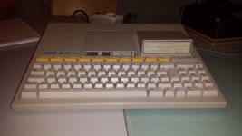
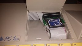
Now I have the same idea in a XT Class PC (Olivetti Prodest PC1 HD). It has a XTA interface, somewhat different (it is the "industry standard" XT-IDE, lacking A2) with "strange" AEN (Attention ENable? = I/O CHRDY? a sort of?).
IRQ 5 is used instead if IRQ 14. Base port 320h

Table 15.8 XT-Bus IDE Connector
1 -RESET
3 Data 7
5 Data 6
7 Data 5
9 Data 4
11 Data 3
13 Data 2
15 Data 1
17 Data 0
19 Ground
21 AEN
23 -IOW
25 -IOR
27 -DACK 3
29 DRQ 3
31 IRQ 5
33 Address 1
35 Address 0
37 -CS1FX
39 -Drive Active

Someone else has tested it? I want to use IDE-XT-CF bios, Should I change IRQ? A2 is strictly necessary? Custom XTIDE Universal BIOS?
In the next days I will try some solution. If it work, would mean no ISA slot waste at all & built in HD.
 
Last edited:
AEN is a standard ISA signal and is usually connected on all ISA cards. All the signals described, with the exception of CS1FX and Drive Active, come straight from the ISA bus. A2 is not needed for classic XT IDE because it only uses addresses 320h-323h. This corresponds exactly to the old Xebec 1210 controller.
 
I want to use IDE-XT-CF bios, Should I change IRQ? A2 is strictly necessary? Custom XTIDE Universal BIOS?
In the next days I will try some solution. If it work, would mean no ISA slot waste at all & built in HD.

IIRC the XTIDE Universal BIOS can live without A2. Someone probably needs to check the register maps (or try it with the line held high at the drive). Some BIOS space would be needed somewhere of course for the XTIDE Universal BIOS (the onboard device BIOS certainly won't work, since it won't issue the commands to set the CompactFlash media to 8-bit operating mode).

Also, DMA & IRQ lines are not used by XTIDE Universal BIOS.
 
So, if I understand, i can Connect "straight" a CF card, cutting line 21, 27, 29, 31 (where is I/O CH RDY???), maybe cutting also line 4, 6, 8, 10, 12, 14, 16, 18 (data 8-15) all the other Lines are in the right position I think...
Then fire in XTIDE bios with 320h-323h range! PIO mode etc etc

Maybe can work!
 
Yes, the minimum connections needed are D0..7, IOR/IOW, IDE_CS0, and Address 0/1. For the address lines, connect CompactFlash A0 and A1 to the PC A0 and A1 and select "8 bit controller in 16 bit slot" in the XTIDE Universal BIOS configuration. Reset line looks to be correct polarity so that could be connected too.

On the CompactFlash end, hold A2 low, IDE_CS1 high, attach 10k pull-up to IORDY, and 10k pull-down to DMARQ and D7.

Hope that helps.
 
After successfully connecting XTA to CF, XTIDEBios set to 8bit, cmd block 320, control block 320??? 324??? No means i think
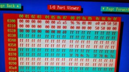
I see the registers in i/o 320-323h, like this "00 00 80 00" with the settings Said above by pierce (A2 low)
That i think are correct valute.
If i do it with A2 high i see in the SAME i/o space: "00 00 00 0d" that if i Remember good are the value of the register XX4-XX7 (in IDE standard 1f4-1f7).
XTIDEBIOS doesn't detect the drive... Ok i'll test in manually... The problem is... How to put the CF in 8 bit mode?

MOV DX,01F1
MOV AL,01
OUT DX,AL
MOV AL,EF
MOV DX,01F7
OUT DX,AL
MOV DX,01F1
IN AL,DX

I can translate 1F1 ->321 but... 1F7???? If i Connect CS3fx i can also see the control block in the SAME space.

I tried to Connect A2 to ISA A2 but with no luck! Only 320-323h register appear!
I miss something?
 
Sorry I made a mistake - it's been a while since looking at this! CompactFlash CS0 is needed, but CS1 we can live without. CompactFlash A0, A1 and A2 are all absolutely needed though and need to be connected to ISA A0, A1, A2 to use the 16-bit adapter in 8-bit slot mode of the XTIDE Universal BIOS.

(Note - there is another option; namely to connect CompactFlash A0, A1 and A2 to ISA A1, A2 and A3 respectively, then select adapter type XT-CF in the configurator.)

CompactFlash CS0 will be driven by the XTA header CS1FX line, CompactFlash CS1 must be held high (these are active-low signals).

In either 16-bit in 8-bit slot mode or XT-CF mode, the XTIDE BIOS will issue the feature-set commands to select 8-bit mode during device initialisation.

Sorry about that :)
 
Last edited:
Ok, Now i got it. And tried. Thank you pearce for your info.
The problem is that when i Connect A2 (cf A2 to ide A2) but Then i got registers 04-07 to 320-323! If a2 disconnetted i got 00-03 registers instead. XTIDE bios need all the registers, so i crucial to have it connected! It seem that cf understand to display the correct register but pc put it in the wrong port like XT side "mask" the A2 line.
Maybe A2 need to be pulled-up or inverted? Or the PC is driving the CS1FX in the wrong way?
Or maybe my XT is blocking port 324-327 for some reason.
Damn!
 
Ah, yes of course.. The address decoder driving the XTA interface (CS1FX specifically) no doubt is matching A2..A9 against C8h (320h >> 2). You need to find that chip and disconnect A2 from it - if the chip is socketed, pull it, angle out the appropriate pin, re-insert and then tie that pin low (to ground).
 
Hoooray, registers are up & running. I find the right chip that was luckily socketed! Grounded the pin Then I had a spare A2 line to use connected to cf/ide adapter ;). All register are Now there! (But What a pain reach here!)
Now image.jpg
Register are correct i think (i Remember the same values from a 16bit adapter...) but the cf is unrecognized (it is good in XTIDE adapter instead). Register seem to be somewhat 'static', Or "read only".
NeXT time I'll try some ATA command to see.
Just for the first try i disconnetted d08-d15 iochrdy drq3 dack3 irq cs3fx... Maybe one if theese. I'll try cs3fx to high as suggested. Now is late (in italy).
 
Good news! Did you change the IO base address in the BIOS to 320h? CS3FX (CompactFlash CS1) needs to be held high certainly. But the BIOS should now find the media.
 
No go for Now... I see all the register, but it seem that i cannot modify (write) to it. BIOS does not detect.

IO base address is correct, CS1 to high (verified), also connected IRQ to IRQ5, DRQ3, DACK3, every single action verified by IO write, but no change at all in the register. CF good, tried 3 different (all working in XTIDE same PC),
connections are good because i tried the very same connector in XTIDE with only A0, A1, A2. & D0-D7 & IOR IOW & CS1FX and the card is RECOGNIZED! (But no boot) CS3FX was simply disconnetted.
Considering that the connections are all ISA except 1... The problem must be CS1FX... for sure.
The procedure for writing to IO port are the same for reading? (Only reversing IOW/IOR I imagine). Maybe the build in address decoder doesn't work for some strange reason?


(Also tried your master/slave bios! I'll write in the other thread :) )
 
The way it works is: the address lines (A3..A9 in this case, with the mod in place) are matched by the decoder, causing an active-low output that appears on the header at pin 37. After a clock cycle, either: Data appears on the data bus and IOW is then asserted low, OR IOR is asserted low and data is loaded from the device.

I have a few thoughts:

  • IDE_CS1 needs to be held high, as otherwise it's logic level will basically be whatever the result of surrounding noise provides
  • What's happening with the CF media reset line? That should be tied to the XTA header reset, since both are active LOW.
  • Possibly (but seems unlikely), the bus transceiver isn't achieving CMOS spec logic levels at the CF media. You could try changing the CF supply to 3V3.
  • There is presumably a bus transceiver in the circuit (probably 74LS245N), possibly dedicated to the XTA interface? You can find it by following back the data lines from the header. We need to confirm what drives it's OE pin (hopefully the address decoder output) and it's direction pin (hopefully just ISA IOR).
  • INTRQ, DMARQ and DMACK aren't needed for operation, but DMARQ should have 10k PD connected

Other than that, I can't think why it's not responding to writes - it's very puzzling. I feel it could be related to the comment at the top of this page,

when i Connect A2 (cf A2 to ide A2) but Then i got registers 04-07 to 320-323! If a2 disconnetted i got 00-03 registers instead

I can't figure that out.... unless there was a mistake and CF A2 ended up hooked up to some other line or just Vcc?
 
* IDE_CS1 held high
* Reset line connected
* maybe is a transceiver is the problem so the result would be very difficult.
* DMARQ was left unconnected

BUT the same configuration worked when connected to XT-CF card also with DMARQ disconnected

The next time I'll try:
1) Connect the ide cf to XTA interface EXCEPT CS1FX that i'll Connect to XT-CF line. If it work all line are good except CS1FX
2) Connect the ide cf to XT-CF interface EXCEPT CS1FX that i'll Connect to XTA line. If it work CS1FX is driven right and something is wrong in the other Lines (but theese are all ISA double... at least my tester said so)
2) I think -reset is not the problem because prior to disconnect a2 from the address decoder i seen different value on 320-323 so the CF card was working, also in writing...
3) maybe is the address decoder the problem. Must the disconnected pin "tied to low" to show 320-327 registers... But in Reading mode, should be the same?

new misteries await! ;)
 
Good news! I think you are the first to get CompactFlash running from an onboard XTA physical interface :)
 
Back
Top