• Please review our updated Terms and Rules here

Compaq Portable II, Recreating the 512/1536 Kbyte System Memory Board (104176-001)

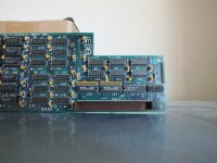
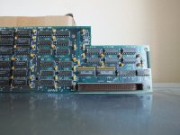
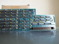
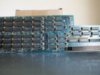
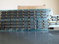
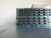
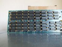
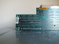
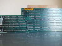
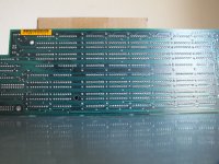
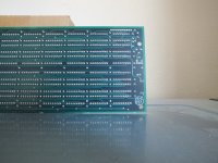
Hey @btb finally catching up on some things and I saw your comment on my CP3 vid, just checking in here to put my support behind it all! Amazing to see some photos of an original unit, esp considering how basically non existent info is about them.. probably the first photos of one on online!

I'm very much on board with whatever help you need, great progress so far. I could take that and reproduce it in Kicad etc if need be, or alternately happy to test if you're already way ahead of me. Just let me know!
 
Do you need any more pictures? If not, I'll install it back on my Portable II. The stand offs aren't in bad shape, but almost 40 year old plastic is getting brittle, I don't want to remove/re-install it too many times if I don't have to.
These are amazing and thank you so much! If still possible, and this is very big ask, could we get two more things?

Most importantly, precise dimensions of the overall width and height, and ideally of that cutout area?
If possible also the stand-off and connector locations as anchor points. Getting those accurate in a reproduction will be crucial

I'd also like to do a full high quality photomerge of the final board as well - would you be able to take a bunch of photos just scanning over the board left to right? As many as possible! The perspective on the current photos makes merging them together a bit warped
I'll see what I can do for the top of the board, but the bottom scans should be consistent angle, and are at 300 dpi, so may be good for dimensions.

I'll go out to my shop tomorrow and get my calipers, that will let me take the most accurate measurements. I'll try to get the center of the mounting holes to their nearest square edges, and the big header connector from both edges of the board.
 
I'll re-do the bottom scans with it held straight against an edge, spaced away from the top edge so we get the top of the board.

But a quick check does show the board is about 3.73 inches in the narrow dimension, which matches the around 1120 pixels wide of the scan at 300dpi.
 
I'll see what I can do for the top of the board, but the bottom scans should be consistent angle, and are at 300 dpi, so may be good for dimensions.
Oh yep sorry, the bottom photos are great for seeing the traces, but missing the very edges so dimensions would be ever slightly off.

I'll go out to my shop tomorrow and get my calipers, that will let me take the most accurate measurements. I'll try to get the center of the mounting holes to their nearest square edges, and the big header connector from both edges of the board.
That'd be excellent, thank you very much!

Down the line, might need your assistance if you can provide tracing some of the pin contacts down the line. Just looking at the photos and the traces that snake underneath some parts and the header connector in particular are going to be somewhat guessable but not everything.
Best case scenario would be removing all the components and imaging the board like that, but definitely understand why that may not be an option esp given the rarity!
 
R3 has one trace that connects to both the 74S734 and 74F32, and the other side is connected to ground (pulling these pins low I assume).

On R9/R10 the leads without traces connect R9 to R10 (these connect to the positive plane, they are pulling a pin high on one 41256 in each bank). One of these connects to pin B 12 on the interface connector.

This may be a sense line of some kind. There is also a connection between ground and A5. This may also be a sense connection On the back side of the board you'll see a1/b1 and b26 labelled.

I'd rather not destroy this board, as it is original to my system.
 
Last edited:
We have another plane in this board, a positive plane. The bypass caps have no visible traces, but when shown through with a flashlight show cross shaped traces on each side.
 
Yeah, we can do it without removing anything. If you’re able to provide a handful more connections that will probably do it. I have a schematic and a kicad layout in progress. My plan is to make a new one that uses SIMMs, but someone might want the original footprint as well.

Those little capacitors really say 475 on them? 4.7uF seems like a lot for a bypass cap, but maybe these DRAM chips need that oomph, I dunno.
 
That's great that you found some chips to fill up your board. You'll want to set the MS3 jumper on your motherboard to the "1.5" or "G" position.
If you also have an ISA memory board you'll need to tell it to start at 2.5MB rather than 2MB

Do the v5 or the v8 diagnostics disks check all the ram accurately for you?
I have a later revision and may not need to change the jumper as the memory size is controlled by the setup program, I decided to reassemble my Portable II for now without the memory expansion and I had to re-run setup to set the memory size to 640k. The manual says that MS3 is set to 1536k by default.

All of the caps on the board are bypass caps, they all connect to the ground and power plane. The layers are component / ground plane / power plane / back.

The standoffs might be 3d printable to make replacements...
 
I have a schematic and a kicad layout in progress. My plan is to make a new one that uses SIMMs, but someone might want the original footprint as well.
I would like to make as close to a 1:1 reproduction as I can, but I'm happy to take your lead for the rest. If you already have a bunch of work done, I'd rather not have to redo a bunch of schematic repro... maybe share the files in a Git repo for collab?

Those little capacitors really say 475 on them?
The photos are a bit blurry, but they look like 473 to me and 47nF makes a lot more sense. It's also the same value used for DRAM bypass on the CP2 itself (attached) and the CP3 expansion board for that matter20240323_102603.jpg
 
Last edited:
  • Like
Reactions: btb
They do say 473. It's a bit of a hard to read font, and tired eyes last night I guess. Below that is definitely "E5Z"
 
  • Like
Reactions: btb
Dimensions:
Top edge 1: 25.2 cm
Top edge 2: 8.5 cm
Bottom edge: 33.7 cm
Full width: 9.45 cm (verified at both ends and the middle of the wide section)
Width of connector section: 6.55 cm
Verified difference in width measured where the card gets wider: 2.9 cm
Interface connector is 2.0 cm from the right hand edge, 3 mm from the bottom edge, connector base measures 8.45 cm x 9 mm.

I'll re-do the bottom scans making sure it's straight to the edge and away from the top, so they can be stitched together.

Edit: I mismeasured the distance from the connector base to the bottom edge, measuring the silk screen line instead of the connector initially, but I've corrected it.
 
Last edited:
How are these macro shots?
 

Attachments

  • P2 memory card macro 01.jpg
    P2 memory card macro 01.jpg
    1.3 MB · Views: 7
  • P2 memory card macro 02.jpg
    P2 memory card macro 02.jpg
    1.4 MB · Views: 6
  • P2 memory card macro 03.jpg
    P2 memory card macro 03.jpg
    1.4 MB · Views: 6
  • P2 memory card macro 04.jpg
    P2 memory card macro 04.jpg
    1.5 MB · Views: 6
  • P2 memory card macro 05.jpg
    P2 memory card macro 05.jpg
    1.5 MB · Views: 7
  • P2 memory card macro 07.jpg
    P2 memory card macro 07.jpg
    1.2 MB · Views: 7
  • P2 memory card macro 06.jpg
    P2 memory card macro 06.jpg
    1.4 MB · Views: 7
  • P2 memory card macro 08.jpg
    P2 memory card macro 08.jpg
    1.3 MB · Views: 6
  • P2 memory card macro 09.jpg
    P2 memory card macro 09.jpg
    1.5 MB · Views: 6
  • P2 memory card macro 10.jpg
    P2 memory card macro 10.jpg
    1.5 MB · Views: 6
U58 pin 2 and 4 are tied together, then go to the main connector, pin ?
U58 pin 11 goes to?
Connector pin B11 goes to U58 pin ?

C70-C74 all are just VCC and GND also?
Apart from R3, do any of the resistors (present or not) connect to GND, or are they all on VCC?

I'm pretty sure you can still get those standoffs new. They hold the PCBs 7/8" apart?

I'll put the Kicad project up on GitHub shortly.
 
U58 pin 2 and 4 connect to pin B5 (as numbered on the back of the board)
U58 pin 11 connects to U54 pin 9, then goes under U51 to connect to U51 pin 9 as well.
C70-74 aren't populated, have one pin to the ground plane, but have a trace running from them on the other side of the cap.
C70 connects to R5, other side of R5 connects to pin 3 of U1
C71 connects to R4, other side of R4 connects to pin 4 of U1
C72 connects to R8, other side of R8 connects to a via under U4
C73 connects to R6, other side of R6 connects to pin 3 of U7
C74 connects to R7, other side of R7 connects to pin 4 of U7

R1/R2 form a voltage divider, R1 connects to GND, R2 to VCC, they connect to each other and pin 1 of U17.

Looks like C70/R5 and C73/R6 are signal conditioning the WRITE signal and C71/R4 and C74/R7 are conditioning the RAS signal, if they were populated.
 
Last edited:
  • Like
Reactions: btb
Very cool, I basically only have a couple questions left. Everything except the specifics of the logic is worked out since the banks are basically all identical to what's on the motherboard.
where does pin 1 of U57 connect? probably pin 19 or GND?
where does pin 13 of U58 connect? probably B11 on the connector?
 
Pin 1 of U57 connects to pin 19 of U57, which connects to R3 which is 150 ohms to ground.
Pin 13 of U58 does connect to B11 on the connector, it does this with a trace on the top side that drops into a via, then around the back to another via just above B11.
 
  • Like
Reactions: btb
Front photos are good, have some photomerges on the way all perspective corrected and to dimensions provided (having a professional photographer for a partner makes it a cinch ;) )
 
  • Like
Reactions: btb
Back
Top