HoJoPo
Veteran Member
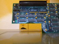
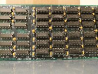
I used the top of my little Engel 63 quart chest freezer to try to keep the camera about the same distance from the card, sliding the camera along one of the seams in the top. Seems to have worked.


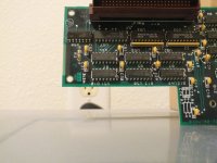
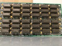
U58 pin 2 and 4 connect to pin B5 (as numbered on the back of the board)
U58 pin 11 connects to U54 pin 9, then goes under U51 to connect to U51 pin 9 as well.
C70-74 aren't populated, have one pin to the ground plane, but have a trace running from them on the other side of the cap.
C70 connects to R5, other side of R5 connects to pin 3 of U1
C71 connects to R4, other side of R4 connects to pin 4 of U1
C72 connects to R8, other side of R8 connects to a via under U4
C73 connects to R6, other side of R6 connects to pin 3 of U7
C74 connects to R7, other side of R7 connects to pin 4 of U7
R1/R2 form a voltage divider, R1 connects to GND, R2 to VCC, they connect to each other and pin 1 of U17.
Looks like C70/R5 and C73/R6 are signal conditioning the WRITE signal and C71/R4 and C74/R7 are conditioning the RAS signal, if they were populated.

So pin 3 of U1 and pin 3 of U7 not shorted together?Minor updates for your schematic:
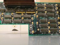
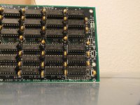
C70 connects to R5, other side of R5 connects to pin 3 of U1 (Bank 4)
C73 connects to R6, other side of R6 connects to pin 3 of U7 (Bank 2)
I mean, it's not wrong in that WE is connected together, but R6 does connect across the board at bank 2, not directly at bank 4.
I'll see if I can verify R8's connection, I may have to pull the chip it goes under with a via.
Yep will do, there's a few tweaks I'd like to make and then do all the particulars around board markings and such, but otherwise it's looking pretty dang perfect. Seriously well done
Question- the trace at the bottom of the board that cuts through the BANK 2 silkscreen is unrouted. I think this might be a separated ~{WE} line for banks 3/4, maybe to keep signal integrity etc. I can't think of anything else that it would connect to there...
View attachment 1276220