• Please review our updated Terms and Rules here

Epson QX10 Endless Beeping (Diagnostic Code 0002)

MattPilz

Member
Joined
May 29, 2019
Messages
12
Location
USA
I've been having a go troubleshooting an Epson QX-10 but know there are some here far more experienced with this system than I am. The problem is immediately on boot it goes into an endless beep with "Diagnostic Code: 0002" shown. It does not reach the point of reading disks or anything else, the system halts.

According to the manual and to a ROM disassembly, error 0002 is indicative of a memory error, rather than CPU. I have tested, swapped and reseated every 4164 chip on the main board and the video board (every bank is full). If I remove the video board from the main board the beeping stops. I also tried replacing the video IC (D7220AD) and the two DMA controllers (D8237AC), as well as the CPU. I have not replaced the CMOS battery. I did also dump and compare/verify the ROM with the one here.

I'm aware of the great collection of documentation at this site but was curious if anyone might have a "next steps" recommendation for troubleshooting this situation.
 
I just purchased a QX-10 after a few decades since I owned one so getting back into this model again and found your post. Are you still having an issue ? If you have a pdf of the QX-10 Operations Manual, look at Appendix G.
It shows how to lower the memory settings by turning dip switch 6 on 7 off 8 on. Try that and see if you get the memory error. If you don't then you would need the diagnostic disk to determine which memory is bad. I think the dip
switch setting lowers the amount of ram that gets tested on boot so the diagnostic program is able to run even with bad upper memory. If the code and beep is still present then the fault would be in the lower banks of ram. You could switch ram between banks if it's socketed. It could be a socket issue rather than a chip

Larry G
 
So that "Diagnostic Code: 0002" should only be generated if there is an issue with the dram for Bank 0 (specifically in the range 0xF000 - 0xFFFF). Unfortunately unlike banks 1-3 which are socketed, I believe bank 0 is soldered directly to the motherboard so you will need the ability to desolder the bad chip from the motherboard.

I can't remember of the top of my head where the Bank 0 i located, but you could probably look for a group of 8 soldered 4164 chips on the motherboard. The trick will be to try and figure out which one(s) are bad so you only have to desolder the correct chips. You might try touching them to see of any are running hot and if not then try the piggyback method with a known good 4164 to see if you can get the system to boot and determine which is one is bad.
 
Thank you both! I had set this project aside and at some point came upon a second QX-10 that had a bad video sub-board but I was able to get it running. However, I'm curious yet to fix the original. I did ultimately socket the bank 0 ones and had hope that would resolve it, since I found a couple bad RAM from that on my tester. The on-board RAM is below the video control board so that needs to be removed to access them.

Unfortunately even that did not resolve that error. Very odd especially given I now have socketed those parts and tested all the RAM. Larry might've been onto something about it being sockets themselves but if it only checks bank 0 then that would be ruled out as I put all new sockets in.

Larry thank you for the dip switch info. I recall doing some adjustments to that switch but grew confused at whatever reference I was reading about it. I look forward to continued troubleshooting of this as it seems the RAM error should be the easier of the two potential errors to figure out. Just being stubborn.

Do you know what diagnostic disk would pair with the QX10? One that can check RAM etc? I do not remember if there was a dedicated QX-10 diag disk or not. Also the floppy drives of these machines seem to be exceptionally fragile and diminished over time. Of the four drives I now have in my arsenal only one is able to read but it may be possible to service them. They all have the little latch that goes up when the disk is inserted that also seems to get stuck nowadays. I have Scott M. Baker's PCBs to build his three custom extensions (Sound Card, Speech Synth and Drive Emulator) but haven't had the time to run the components yet or test that.

I will be sure to update any new findings with the RAM issue, too.
 
Yeah reading the disassembled ROM it seems fairly clear that the Diag 002 message it shown when it fails testing the memory between f000 and ffff and that should always be the bank 0 ram. The top 8k of ram is common and can't be banked out on the QX-10 since that is where the bios is loaded into memory. If you have socketed new known good dram for bank 0 then it seems likely it might be an issue with one of the surrounding logic chips that handles memory access being possibly bad.

If you can find a copy of the Sams COMPUTERFACTS for the Epson QX-10 that would be helpful since it contains a set of complete schematics for the machine. I have a copy i bought some time back, but I'm not sure how easily it is to find one now. You might at least try to look at the current DRAM chips with a scope while booting to see if the control/address signals going to the chips look reasonably sane, though the fact that they are covered by the video board makes that harder.

The Diag disk used for the QX-10 can be found here. It is in the DonMaslin set. It will do a full check RAM check of banks 0 - 3 and will even inform you of which chips are bad in a given bank, though you do need to be able to boot from a floppy first. I've actually used it to find a bad chip in one of my QX-10s before.

Yeah the drives can be an issue on this sometimes, the eject mechanism/latch is usally fairly easy to fix if you clean and reapply some light machine oil to it though.
 
Thanks, I did actually buy a copy of the SAMs QX-10 schematic (digital) toward the very tail end of my troubleshooting when I discovered such a thing existed! I printed it out but haven't gone through it too carefully. I bet you're right and it's an error somewhere up the line from the on-board RAM.

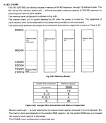
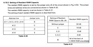
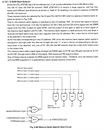
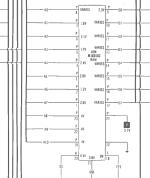
I see from the SAMs schematic the RAM most directly feeds through SN74S257N chips. Attached are a couple potentially relevant grabs from the original service manual, too.
1667840110492.png


1667840445656.png1667840540395.png1667840607362.png
 
So I had been wondering if perhaps the resident RAM was maybe not part of the dram banks to begin with. Looking at what you included from the service manual that might be the case, if you look at Fig 4-63 it appears that circuit will only select a bank of dram if among other things the resident RAM is not selected. Since the signal on pin 13 of 22F would have to be high.

I think i would try go look over the schematic and try to find the resident ram signal on that to see if you can find out what RAM is activated when it is low. We know it should be an input to 22F and elsewhere in the service manual it looks like it is generated by chip 8K on pin 8, tracing where that signal might show that there is a separate memory module used for resident RAM that might be the actual bad memory in your system.
 
I can't remember if I found or adjusted J4 as I also still don't fully understand the resident RAM part or purposes.

It does use a HD146818P for "Real-time Clock Plus RAM" (which I read in datasheet is 50 bytes low-power static RAM). And what SAMs identifies as M16010C RAM, seen below. I can't even find a datasheet for that chip.

1667878578920.png
 
Ok so the resident RAM (Also referred to as common RAM in some documents) is basically the RAM that is always mapped into memory irregardless of what bank is actually selected. The default jumpers are set to E and D giving 8k of resident RAM. This is needed because regardless of which bank is currently selected we need some ram that contains the BIOS so that it is always accessible.

The M16010C SRAM is the 2k CMOS RAM, an alternative part number which does have a datasheet for it is the NEC UPD449.

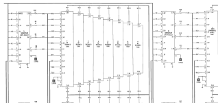
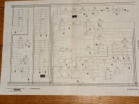
I did some looking through my schematics at where the QX-10 does memory selection. The black circle with a dot in it is highlighting a mistake on the schematics (The SAM's schematics are useful but not without errors). Basically there should be a junction there otherwise nothing is driving the input of 22F pin 13 or 18H pin 2. Both of those should be driven by the UU signal, which is the active low signal that tells us the resident RAM is being selected.

Now looking further at this I have come to the conclusion that i was right first time bank 0 is used as the resident RAM area, that is if you are accessing any address in your resident ram area bank 0 is going to be selected regardless of what bank is selected via the banking register. The important think to note is that is the four /RAS[1-4] signals that ultimately select a bank for access. These are created with a 4 NAND gates all of them take the common active high RAS and PRI signals and combine them with one of the M[7-10] signals, with M7 representing bank 0.

On the right side of the attached schematic we can see that M is being generated by 18H which is a 3 input NAND gate, the three inputs are the /RFSH signal, the Bank 0 select signal (19F pin 4 output) and finally the UU signal which is the active low resident RAM select signal. So ultimately the M7 (active high) will end up being activated during a dram refresh, if bank 0 is selected via IO address 0x18, or if you are accessing the resident RAM area.

What this all means is that use the bank 0 ram is indeed what is being access by the IPL ROM and is giving you the Diag 002 message, so yeah if you have replaced and socked it with known good DRAM it shold not be the actually DRAM that is he issue but with control signals somewhere. I might start be using a scope to look at the inputs and outputs of 18H that are used to generate the M7 signal. You should use the input Pin 2 go low whenever accessing accessing the resident RAM and this should in turn cause pin 12 to be high. I suppose the refresh circuit by have an issue as well so checking to see if pin 13 never goes low might be useful as well.
 

Attachments

  • qx-10_schematic.jpg
    qx-10_schematic.jpg
    2.5 MB · Views: 7
Back
Top