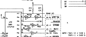
Hey, need some help getting my recently acquired kaypro 4 (m81-240 motherboard) working. Seems to power up ok, but the screen is just filled with a bunch of garbage. I have already pulled all the socketed chips and tested them out, they all tested good and are now replaced. I have removed the monitor rom and replaced it with a blank 2732. So when I power it up it just executes RST 38h's, filling up memory with 0x0039. I also took out U82 - disk controller, u54 pio, u72 pio, and u70 sio since they were all on the unbuffered bus. I have been poking around on u60 (75ls138 responsible for generating the enable signals for the rom and the video ram) with my logic analyzer and everything looks ok except that it looks like G1 on the chip (pin 6) is always staying high. From the 81-241 schematics it shows that this pin is driven by a signal called '(B)BANK'. for the life of me I can't find what is driving this line in the schematics. The (B) indicates that is on the B sheet of the schematics (the IO sheet) but I can't find it there or any circuitry that looks like it would generate it.
I have looked through the kaypro II theory of operation but there seem to be some disconnects between the schematic and the narrative.
Any help with finding where this signal comes from would be greatly appreciated as I think this is either the root of my problem or pretty darn close to it.
Of course, any other suggestions would also be appreciated.
Thanks!